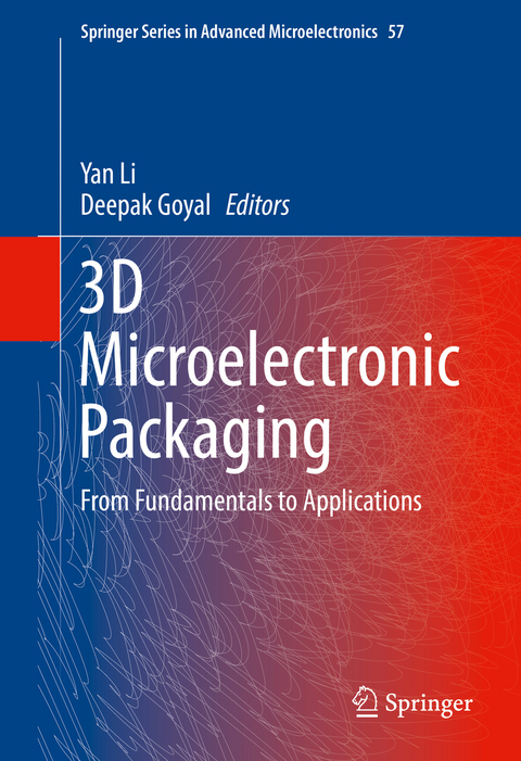
3D Microelectronic Packaging (eBook)
IX, 463 Seiten
Springer International Publishing (Verlag)
978-3-319-44586-1 (ISBN)
Contents 6
Contributors 8
About the Authors 10
Chapter 1: Introduction to 3D Microelectronic Packaging 11
1.1 Introduction 11
1.2 Why 3D Packaging 13
1.2.1 Moore´s Law 13
1.2.2 Small Form Factor Requires 3D Packaging 14
1.2.3 Improved System Performance with Reduced Power 15
1.3 3D Microelectronic Packaging Architectures 16
1.3.1 Die-to-Die 3D Integration 16
1.3.2 Package-to-Package 3D Integration 19
1.3.3 Heterogeneous 3D Integration 19
1.4 3D Microelectronic Packaging Challenges 21
1.4.1 Assembly Process, Yield, Test, and Cost Challenges 21
1.4.2 Thermal Management, Package Design, and Modeling Challenges 21
1.4.3 Material and Substrate Challenges 22
1.4.4 Quality, Reliability, and Failure Analysis Challenges 22
1.4.5 Summary 23
References 24
Chapter 2: 3D Packaging Architectures and Assembly Process Design 26
2.1 Introduction 27
2.2 3D TSV-Based Architectures: Advantages and Limitations 34
2.3 Methods of Fabrication and Other TSV Attributes 39
2.4 Assembly Process Flows 44
2.5 Manufacturing Yields and the Role of Test 48
2.6 Challenges with 3D TSV Architectures 51
2.7 Summary 52
References 52
Chapter 3: Materials and Processing of TSV 56
3.1 Introduction 56
3.2 Overview of TSV Materials and Processes 57
3.3 Fabrication of TSV and TSV Assembly 58
3.3.1 Creating a Via or Trench in Si Wafer 59
3.3.1.1 Laser Drilling 60
3.3.1.2 Powder Blast Micromachining 61
3.3.1.3 Wet Etching 62
3.3.1.4 Plasma-Based Methods 63
3.3.2 Sequential Filling of Si Via 66
3.3.3 Planarization and Die-Thinning 70
3.4 Flow Process for Fabricating TSVs and Integration of Dies 71
3.4.1 Sequence of Flow Process 71
3.4.2 Integration of Dies Comprising TSVs 73
3.5 Summary 74
References 75
Chapter 4: Microstructural and Reliability Issues of TSV 79
4.1 Introduction 79
4.2 Microstructural Characterization and Stress Measurement 80
4.2.1 Microstructural Characterization 80
4.2.2 Measurement of Stress State 82
4.2.2.1 Wafer Curvature Method 82
4.2.2.2 Micro-Raman Spectroscopy 83
4.2.2.3 X-Ray Diffraction-Based Techniques 84
4.2.2.4 Stress Metrology Challenges 85
4.3 Reliability Issues Associated with TSVs 85
4.3.1 Stresses in TSVs 85
4.3.1.1 Origin and Effect of Stresses 85
4.3.1.2 Microstructure and Stresses 89
4.3.1.3 Metal Pumping: Extrusion or Intrusion of TSVs 91
4.3.2 Electromigration Related Effects 96
4.4 Towards Atomistically informed Reliability Modeling of TSVs 99
4.4.1 The CPFE Method 99
4.4.2 The PFC Method 100
4.5 Summary 102
References 103
Chapter 5: Fundamentals and Failures in Die Preparation for 3D Packaging 108
5.1 Introduction 108
5.2 Brief Overview of TSV Wafer Fabrication Processes 109
5.3 Wafer Buckling and Wrinkling 115
5.4 Thermal Sliding Wafer Debonding 117
5.5 Wafer Laser Scribe 121
5.6 Wafer Saw Process 124
5.7 Wafer Die Ejector 129
5.8 Conclusions 131
References 132
Chapter 6: Direct Cu to Cu Bonding and Other Alternative Bonding Techniques in 3D Packaging 136
6.1 Introduction 136
6.2 Solder-Based vs. Solder-Less Bonding: Pros and Cons 137
6.3 Stacking and Bonding Schemes, Technologies, and Applications 139
6.4 Thermo-Compression Bonding (Diffusion Bonding): Material Fundamentals and Microstructure Effects 140
6.5 Passivation with Capping Layers (SAMs and Metals) 143
6.6 Surface Activated Bonding (SAB) Processes 144
6.6.1 Cu/Dielectric Hybrid Bonding 148
6.6.2 Cu/SiO2 Hybrid Bonding 149
6.6.3 Cu/Adhesive Hybrid Bonding 153
6.7 Alternative Bonding Techniques: Insertion Bonding 155
6.8 Cu-Cu Bonding: Equipment Landscape and State of the Art 157
6.9 Chapter Summary and Future Recommendations 157
References 158
Chapter 7: Fundamentals of Thermal Compression Bonding Technology and Process Materials for 2.5/3D Packages 163
7.1 Introduction 163
7.2 Background 164
7.2.1 Overview of 3D Package Configuration 165
7.2.2 Fundamentals of Thermal Compression Bonding Technology 168
7.2.2.1 Technical Challenges of Mass Reflow Process Compared with TCB 168
7.2.2.2 Thermal Compression Bonding Tool 172
7.2.2.3 Thermal Compression Bonding Process 174
7.2.3 Fundamentals of Process Materials 179
7.2.3.1 Introduction 179
7.2.3.2 Basic Properties Measurement 179
7.2.3.3 Wetting Study 183
7.2.3.4 Void Formation Study 185
7.3 Principles of Materials Formulation 186
7.3.1 Water-Soluble Flux 187
7.3.2 No-Clean Flux 188
7.3.3 Capillary Underfill 189
7.3.4 Epoxy Flux (No-Flow Underfill or Non-Conductive Paste) 190
7.3.5 Pre-Applied Epoxy-Based Materials (Non-Conductive Film and B-Stage Material) 192
7.4 Assembly Process Design 195
7.4.1 Introduction 195
7.4.2 TCB Assembly Building Block 196
7.4.3 TCB Assembly Building Block Design and Development 198
7.4.3.1 TSV Memory Stacking 199
7.4.3.2 Memory Module to Logic or Silicon Interposer Attachment 203
7.5 Summary and Discussion 206
References 207
Chapter 8: Fundamentals of Solder Alloys in 3D Packaging 210
8.1 The Microbumping Process 210
8.2 The Solder Alloys in Microbump 215
8.3 The Formation of Intermetallic Compounds in the As-Produced Microbump 215
8.4 Microstructure Variation of Microbump Under Thermal Mechanical Conditions 220
8.5 The Microstructure and Failure Mechanism of Microbump 222
8.6 Summary and Future Challenge 224
References 225
Chapter 9: Fundamentals of Electromigration in Interconnects of 3D Packaging 228
9.1 Introduction 228
9.2 Key Modulators for EM in Solder Joints 229
9.2.1 Typical EM Fail Caused by Sn Diffusion 229
9.2.2 EM Fail Caused by Metallization Dissolution 232
9.3 EM in Solder Joints of 3D Packaging 237
9.3.1 EM Damage due to Sn Flux Divergence in Micro Bumps 237
9.3.2 The Transformation of Full IMC Joint Under EM 238
9.3.3 Thermomigration Accompanied by EM 241
9.4 EM in TSV of 3D Packaging 243
9.4.1 EM for Cu Damascene Interconnects 244
9.4.2 EM Failure in TSV 245
9.5 Summary 247
References 248
Chapter 10: Fundamentals of Heat Dissipation in 3D IC Packaging 250
10.1 Introduction 250
10.2 Thermal Performance Parameters for 3D ICs 251
10.3 Air Cooling of 3D ICs 253
10.4 Jet Impingement and Spray Cooling 254
10.5 Microchannel Cooling 254
10.6 Thermal Design Considerations in 3D IC Architectures 255
10.6.1 Thermal Considerations in TSV Placements 257
10.6.2 Thermal Analysis Tools for 3D ICs 257
10.6.3 Performance Considerations 257
10.7 Liquid Cooling with Integrated Microchannels 258
10.7.1 Variable Fin Density in Microchannel Passages 258
10.7.2 Two-Phase Cooling 262
10.8 Future Directions 262
References 263
Chapter 11: Fundamentals of Advanced Materials and Processes in Organic Substrate Technology 266
11.1 Introduction 266
11.2 Overview of Substrate Technology Evolution 267
11.3 Organic Substrate Materials 267
11.3.1 Materials Employed in Organic Substrate Production 267
11.3.2 General Considerations 269
11.3.3 Substrate and PWB Cores 274
11.3.3.1 Reinforcement Materials 275
11.3.3.2 Resin Systems 278
11.3.3.3 Conductors 281
11.3.4 Dielectric Materials 282
11.3.5 PTH and Via Filling Materials 284
11.3.6 Solder Mask Materials 285
11.3.7 Surface Finishes 286
11.3.8 Summary 286
11.4 Organic Substrate Fabrication 289
11.4.1 Substrate Raw Material Selection and Preparation 290
11.4.2 Inner Layer Imaging 292
11.4.3 Multilayer Buildup 292
11.4.4 Soldermask and Surface Finish Application 294
11.4.5 Final Sizing, Testing, Inspection, and Shipment 295
References 295
Chapter 12: Die and Package Level Thermal and Thermal/Moisture Stresses in 3D Packaging: Modeling and Characterization 297
12.1 Introduction 299
12.2 Thermal Stress and Its Effects on TSV Structures 300
12.2.1 Introduction 300
12.2.2 Characteristics of TSV Stress by Semi-analytic and Numerical Solutions 300
12.2.3 Measurement of Thermal Stress 302
12.2.4 Effect of Thermal Stress on Carrier Mobility and Keep-Out Zone 305
12.2.5 Thermal Stress Induced via Extrusion 306
12.3 Thermal Stresses and Warpage Control at Package Level 309
12.3.1 Introduction 309
12.3.2 Thermal Stresses in a Multilayered Structure 310
12.3.3 Warpage Mechanism and Control Methods 312
12.3.4 A Capped-Die Approach for Warpage Control 314
12.3.5 Warpage Characterization by Experimental Testing 315
12.3.6 Numerical Modeling for Optimizing Warpage Control Design 317
12.3.6.1 Comparison of Different Control Methods 317
12.3.6.2 Optimization of Cap Thickness to Achieve Warpage-Free Packages 318
12.3.6.3 Overcontrolled Warpage 319
12.3.6.4 Warpage-Free Control for Coreless Substrate 319
12.4 Integrated Stress Analysis for Combining Moisture and Thermal Effects 321
12.4.1 Introduction 321
12.4.2 Moisture Diffusion 322
12.4.3 Moisture-Induced Strain and Effective Stress Theory 324
12.4.4 Vapor Pressure Modeling 325
12.4.5 Governing Equation for Integrated Stress Analysis 327
12.4.6 Case Studies 327
12.5 Summary 331
References 333
Chapter 13: Processing and Reliability of Solder Interconnections in Stacked Packaging 337
13.1 Introduction 337
13.1.1 Miniaturization and Functionality Trends 337
13.1.2 3D Packaging Variations 339
13.1.3 Applications Drive PoP and PoPoP Component Requirements 340
13.2 Soldering Assembly Processes 341
13.2.1 Solder Alloys 342
13.2.1.1 Sn-Pb Solders 342
13.2.1.2 Pb-Free Solders: ``High Ag´´ Alloys 342
13.2.1.3 Pb-Free Solders: ``Low Ag´´ Alloys 343
13.2.1.4 Mixed Solder Joints 343
13.2.2 Fluxes and Pastes 344
13.2.3 Assembly Methodologies 346
13.2.3.1 Stacked Packages 346
13.2.3.2 Soldering Assembly (Second-Level Interconnections) 348
13.2.3.3 Cleaning Considerations 348
13.2.3.4 Rework 349
13.2.4 Inspection Techniques 350
13.2.5 Underfill, Conformal Coatings, and Encapsulants 352
13.2.5.1 Underfill 352
13.2.5.2 Conformal Coatings 354
13.2.5.3 Encapsulants 355
13.2.6 Warpage Effects 355
13.3 Solder Joint Reliability 358
13.3.1 Environments 358
13.3.1.1 Use Conditions 358
13.3.1.2 Consumer Electronics 359
13.3.1.3 High-Reliability Electronics 360
13.3.1.4 Accelerated Aging 361
13.3.2 Underfill, Conformal Coatings, and Encapsulants 362
13.3.2.1 Materials Properties 362
13.3.2.2 Geometry 363
13.3.3 Reliability Studies 363
13.3.3.1 Mechanical Shock and Vibration 363
Solder Alloy Effects 364
Surface Finish Effects 364
Importance of Test Standards 365
13.3.3.2 Temperature Cycling 365
Temperature Limits 366
Test Vehicle Construction 366
Materials Set for Computational Modeling 367
Solder Alloy Fatigue Properties 367
Effects of Alloy Composition and Underfill on Solder Joint Reliability: An Empirical Study 368
13.4 Summary and Future Trends 373
13.4.1 Summary 373
13.4.2 Future Trends 374
References 375
Chapter 14: Interconnect Quality and Reliability of 3D Packaging 378
14.1 Introduction 378
14.2 Quality Challenges for 3D Packaging 379
14.3 Quality and Reliability of Microbumps 383
14.3.1 Type 1: Cu/Sn/Cu 383
14.3.1.1 Microstructure of Cu-Sn IMCs-Based Microbump 383
14.3.1.2 Microstructural Characteristics of Cu6Sn5 in Microbump 383
14.3.1.3 Kirkendall Void and Porous Void Formation in Cu3Sn 386
14.3.1.4 Anisotropic Effect in Microbump 387
14.3.2 Type 2: Ni/Sn/Ni 391
14.3.3 Type 3: Cu/Sn/Ni 394
14.3.4 Type 4: Cu/Ni/Sn/Ni/Cu 396
14.3.4.1 Typical Composition Parameters of Cu/Ni/Sn/Ni/Cu Microbumps 396
14.3.4.2 IMC/Solder Interfacial Crack Formation 397
14.3.4.3 Ni as Effective Diffusion Barrier to Suppress Kirkendall Void Formation 398
14.3.5 Concluding Remarks 400
14.4 Field Performance Prediction of 3D Packaging 400
14.5 Electromigration Reliability for 3D IC Packaging 402
14.5.1 Introduction on Electromigration 403
14.5.1.1 Back Stress 403
14.5.1.2 Statistical Analysis by Weibull Distribution Function in Reliability Study 404
14.5.2 Experimental Studies of Electromigration in Al and Cu Interconnects 405
14.5.3 Electromigration in Flip Chip Solder Joints 406
14.5.4 System Level Electromigration Studies in 3D IC Packaging 406
14.5.4.1 Electromigration in Microbumps 407
14.5.4.2 Electromigration in TSVs 408
14.5.5 System Level Weak-Link Failure in 2.5D Integrated Circuits 409
14.5.6 Concluding Remarks 412
14.6 Thermomigration in 3D IC Packaging 412
14.6.1 Introduction 412
14.6.2 Fundamentals of Thermomigration 413
14.6.2.1 Traditional TM Studies 413
14.6.3 Thermomigration Studies in 3D IC Packaging 415
14.6.3.1 Thermomigration in Microbumps 415
14.6.3.2 Thermomigration in TSV 417
14.6.3.3 Thermomigration Induced by Thermal Crosstalk 418
14.6.4 Concluding Remarks 418
References 419
Chapter 15: Fault Isolation and Failure Analysis of 3D Packaging 424
15.1 Introduction 424
15.2 Fault Isolation and Failure Analysis Challenges for Advanced 3D Packages 426
15.3 The Application of Nondestructive FI and FA Techniques to 3D Microelectronic Packages 427
15.3.1 Nondestructive Fault Isolation Techniques for Electrical Failures in 3D Microelectronic Packages 427
15.3.1.1 Time-Domain Reflectometry 427
15.3.1.2 Electro Optic Terahertz Pulse Reflectometry 429
15.3.1.3 Lock-in Thermography 431
15.3.1.4 Scanning Superconducting Quantum Interference Device Microscopy 432
15.3.2 High Resolution Non-destructive Imaging Techniques for 3D Microelectronic Packages 434
15.3.2.1 Scanning Acoustic Microscopy 435
15.3.2.2 2D X-Ray Radiography 442
15.3.2.3 3D X-Ray Computed Tomography (CT) 444
15.4 The Application of Sample Preparation and Material Analysis Techniques to 3D Microelectronic Packages 447
15.4.1 Sample Preparation Techniques 447
15.4.1.1 Nanosecond (ns) and Femtosecond (fs) Laser Ablation Techniques 448
15.4.1.2 Plasma Focused Ion Beam (FIB) 448
15.4.1.3 Broad-Beam Argon Ion Milling (EDX) 449
15.4.2 Material Analysis Techniques 449
15.4.2.1 Energy-Dispersive X-ray Spectroscopy (EDX) 450
15.4.2.2 X-ray Photoelectron Spectroscopy (XPS) and Time-of-Flight Secondary Ion Mass Spectrometry (TOF-SIMS) 451
15.4.2.3 Electron Backscatter Diffraction (EBSD) 452
15.5 Failure Analysis Strategies for 3D Packages 454
15.5.1 Understanding the Package Assembly Process, Reliability Stress, and Failure Rate Distribution 454
15.5.2 Efficient FI-FA Flow to Identify Defects 456
15.5.3 In-Depth Failure Mechanism and Root Cause Understanding to Provide Solution Paths 458
15.6 Conclusions 459
References 460
Index 463
| Erscheint lt. Verlag | 20.1.2017 |
|---|---|
| Reihe/Serie | Springer Series in Advanced Microelectronics | Springer Series in Advanced Microelectronics |
| Zusatzinfo | IX, 463 p. 331 illus., 253 illus. in color. |
| Verlagsort | Cham |
| Sprache | englisch |
| Themenwelt | Technik ► Elektrotechnik / Energietechnik |
| Technik ► Maschinenbau | |
| Schlagworte | 3D microelectronic packages • Advanced materials in 3D packages • Failure analysis microelectronic packaging • Heat dissipation • Metallic and polymeric packaging materials • Micro bumps • Quality and Reliability of 3D Packaging • Solder connects in 3D packages • Through-Silicon Via • TSV Processing and Reliability |
| ISBN-10 | 3-319-44586-3 / 3319445863 |
| ISBN-13 | 978-3-319-44586-1 / 9783319445861 |
| Informationen gemäß Produktsicherheitsverordnung (GPSR) | |
| Haben Sie eine Frage zum Produkt? |
DRM: Digitales Wasserzeichen
Dieses eBook enthält ein digitales Wasserzeichen und ist damit für Sie personalisiert. Bei einer missbräuchlichen Weitergabe des eBooks an Dritte ist eine Rückverfolgung an die Quelle möglich.
Dateiformat: PDF (Portable Document Format)
Mit einem festen Seitenlayout eignet sich die PDF besonders für Fachbücher mit Spalten, Tabellen und Abbildungen. Eine PDF kann auf fast allen Geräten angezeigt werden, ist aber für kleine Displays (Smartphone, eReader) nur eingeschränkt geeignet.
Systemvoraussetzungen:
PC/Mac: Mit einem PC oder Mac können Sie dieses eBook lesen. Sie benötigen dafür einen PDF-Viewer - z.B. den Adobe Reader oder Adobe Digital Editions.
eReader: Dieses eBook kann mit (fast) allen eBook-Readern gelesen werden. Mit dem amazon-Kindle ist es aber nicht kompatibel.
Smartphone/Tablet: Egal ob Apple oder Android, dieses eBook können Sie lesen. Sie benötigen dafür einen PDF-Viewer - z.B. die kostenlose Adobe Digital Editions-App.
Buying eBooks from abroad
For tax law reasons we can sell eBooks just within Germany and Switzerland. Regrettably we cannot fulfill eBook-orders from other countries.
aus dem Bereich
