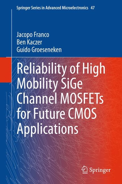
Reliability of High Mobility SiGe Channel MOSFETs for Future CMOS Applications (eBook)
XIX, 187 Seiten
Springer Netherland (Verlag)
9789400776630 (ISBN)
Due to the ever increasing electric fields in scaled CMOS devices, reliability is becoming a showstopper for further scaled technology nodes. Although several groups have already demonstrated functional Si channel devices with aggressively scaled Equivalent Oxide Thickness (EOT) down to 5Å, a 10 year reliable device operation cannot be guaranteed anymore due to severe Negative Bias Temperature Instability.
This book focuses on the reliability of the novel (Si)Ge channel quantum well pMOSFET technology. This technology is being considered for possible implementation in next CMOS technology nodes, thanks to its benefit in terms of carrier mobility and device threshold voltage tuning. We observe that it also opens a degree of freedom for device reliability optimization. By properly tuning the device gate stack, sufficiently reliable ultra-thin EOT devices with a 10 years lifetime at operating conditions are demonstrated.
The extensive experimental datasets collected on a variety of processed 300mm wafers and presented here show the reliability improvement to be process - and architecture-independent and, as such, readily transferable to advanced device architectures as Tri-Gate (finFET) devices. We propose a physical model to understand the intrinsically superior reliability of the MOS system consisting of a Ge-based channel and a SiO2/HfO2 dielectric stack.
The improved reliability properties here discussed strongly support (Si)Ge technology as a clear frontrunner for future CMOS technology nodes.
Jacopo Franco received the M.Sc. in Electronic Engineering from Università della Calabria, Italy, in 2008 and the Ph.D. degree in Engineering from the KU Leuven, Belgium, in 2013. He is currently a Researcher in the reliability group of imec, Leuven, Belgium. His research interests focus on the reliability of high-mobility channel transistors for future CMOS nodes and on variability issues in nanoscale devices. He has co-authored more than 70 papers in international journal and conference proceedings and received the Best Student Paper Award at SISC (2009), the EDS Ph.D. Student Fellowship (2012), the EDS Paul Rappaport Award (2011), and the Best Paper Award at IRPS (2012).
Ben Kaczer is a Principal Scientist at imec, Belgium. He received the M.S. degree in Physical Electronics from Charles University, Prague, in 1992 and the M.S. and Ph.D. degrees in Physics from The Ohio State University, in 1996 and 1998, respectively. In 1998 he joined the reliability group of imec. He has co-authored more than 300 papers and received 5 Best or Outstanding IRPS and 1 IPFA Paper Awards. He is currently serving on the IEEE T. Electron Dev. Editorial Board.
Guido Groeseneken received the M.Sc. degree in 1980 and the Ph.D degree in applied sciences in 1986, both from the KU Leuven, Belgium. In 1987 he joined the R&D Laboratory of imec, Leuven, Belgium, where he is responsible for research in reliability physics for deep submicron CMOS technologies and in nanotechnology for post-CMOS applications. Since 2001 he is Professor at the KU Leuven, where he is Program Director of the Master in Nanoscience and Nanotechnology and coordinating a European Erasmus Mundus Master program in Nanoscience and nanotechnology. He became an IEEE Fellow in 2005 and an IMEC Fellow in 2007.
Due to the ever increasing electric fields in scaled CMOS devices, reliability is becoming a showstopper for further scaled technology nodes. Although several groups have already demonstrated functional Si channel devices with aggressively scaled Equivalent Oxide Thickness (EOT) down to 5A, a 10 year reliable device operation cannot be guaranteed anymore due to severe Negative Bias Temperature Instability.This book focuses on the reliability of the novel (Si)Ge channel quantum well pMOSFET technology. This technology is being considered for possible implementation in next CMOS technology nodes, thanks to its benefit in terms of carrier mobility and device threshold voltage tuning. We observe that it also opens a degree of freedom for device reliability optimization. By properly tuning the device gate stack, sufficiently reliable ultra-thin EOT devices with a 10 years lifetime at operating conditions are demonstrated.The extensive experimental datasets collected on a variety of processed 300mm wafers and presented here show the reliability improvement to be process - and architecture-independent and, as such, readily transferable to advanced device architectures as Tri-Gate (finFET) devices. We propose a physical model to understand the intrinsically superior reliability of the MOS system consisting of a Ge-based channel and a SiO2/HfO2 dielectric stack.The improved reliability properties here discussed strongly support (Si)Ge technology as a clear frontrunner for future CMOS technology nodes.
Jacopo Franco received the M.Sc. in Electronic Engineering from Università della Calabria, Italy, in 2008 and the Ph.D. degree in Engineering from the KU Leuven, Belgium, in 2013. He is currently a Researcher in the reliability group of imec, Leuven, Belgium. His research interests focus on the reliability of high-mobility channel transistors for future CMOS nodes and on variability issues in nanoscale devices. He has co-authored more than 70 papers in international journal and conference proceedings and received the Best Student Paper Award at SISC (2009), the EDS Ph.D. Student Fellowship (2012), the EDS Paul Rappaport Award (2011), and the Best Paper Award at IRPS (2012).Ben Kaczer is a Principal Scientist at imec, Belgium. He received the M.S. degree in Physical Electronics from Charles University, Prague, in 1992 and the M.S. and Ph.D. degrees in Physics from The Ohio State University, in 1996 and 1998, respectively. In 1998 he joined the reliability group of imec. He has co-authored more than 300 papers and received 5 Best or Outstanding IRPS and 1 IPFA Paper Awards. He is currently serving on the IEEE T. Electron Dev. Editorial Board.Guido Groeseneken received the M.Sc. degree in 1980 and the Ph.D degree in applied sciences in 1986, both from the KU Leuven, Belgium. In 1987 he joined the R&D Laboratory of imec, Leuven, Belgium, where he is responsible for research in reliability physics for deep submicron CMOS technologies and in nanotechnology for post-CMOS applications. Since 2001 he is Professor at the KU Leuven, where he is Program Director of the Master in Nanoscience and Nanotechnology and coordinating a European Erasmus Mundus Master program in Nanoscience and nanotechnology. He became an IEEE Fellow in 2005 and an IMEC Fellow in 2007.
Chapter 1: Introduction. 1.1 CMOS scaling: evolutionary era. 1.2 CMOS scaling: revolutionary era. 1.3 High mobility channels for future CMOS technology nodes. 1.4 Reliability limitations. 1.5 Variability issues. 1.6 Objectives and structure of this work. 1.7 Summary of this Chapter. References. Chapter 2: Degradation mechanisms. 2.1 Introduction. 2.2 Negative Bias Temperature Instability (NBTI). 2.3 Hot Carriers. 2.4 Time Dependent Dielectric Breakdown. 2.5 Summary of this Chapter. References. Chapter 3: Techniques and devices. 3.1 Introduction. 3.2 Advanced NBTI measurement techniques. 3.3 Techniques and methodologies used in this work. 3.4 Devices used in this work. 3.5 Structures used in this work. 3.6 Summary of this Chapter. References. Chapter 4: Negative Bias Temperature Instability in (Si)Ge pMOSFETs. 4.1 Introduction. 4.2 Impact of the individual gate stack parameters. 4.3 Gate stack optimization: demonstrating sufficient NBTI reliability at UT-EOT. 4.4 Process- and architecture-independent results. 4.5 Detailed discussion of the experimental results. 4.6 Body Bias and NBTI. 4.7 Model. 4.8 Final considerations: performance vs. reliability. 4.9 Summary of this Chapter. References. Chapter 5: Negative Bias Temperature Instability in nanoscale devices. 5.1 Introduction. 5.2 NBTI on nanoscale SiGe devices. 5.3 Implications for the time-dependent variability. 5.4 Model. 5.5 Impact of Single Charged Gate Oxide Defects: Area scaling. 5.6 Impact of single charged gate oxide defects on the entire FET current characteristics: VG-dependence. 5.7 Impact of single charged gate oxide defects:body bias dependence. 5.8 Summary of this Chapter. References. Chapter 6: Channel Hot Carriers and other reliability mechanisms. 6.1 Introduction. 6.2 Experimental methodology for studying the interplay of CHC and NBTI. 6.3 Interaction of CHC and NBTI in pMOSFETs. 6.4 CHC in SiGe pMOSFETs. 6.5 CHC in Ge pMOSFETs. 6.6 Other reliability mechanisms. 6.7 Summary of this Chapter. References. Chapter 7: Conclusions and perspectives. 7.1 Conclusions. 7.2 Perspectives.
| Erscheint lt. Verlag | 19.10.2013 |
|---|---|
| Reihe/Serie | Springer Series in Advanced Microelectronics | Springer Series in Advanced Microelectronics |
| Zusatzinfo | XIX, 187 p. 219 illus. |
| Verlagsort | Dordrecht |
| Sprache | englisch |
| Themenwelt | Naturwissenschaften ► Physik / Astronomie ► Atom- / Kern- / Molekularphysik |
| Naturwissenschaften ► Physik / Astronomie ► Elektrodynamik | |
| Technik ► Elektrotechnik / Energietechnik | |
| Technik ► Maschinenbau | |
| Schlagworte | Channel Hot Carriers • CMOS Technology Nodes • Design Optimization • device reliability • Electron Device Reliability • High-mobility channel pMOS • Low Frequency Noise • Nanoscale Devices • Negative Bias Temperature Instability • RAN • Random Telegraph Noise (RTN) • Semiconductor Devices • SiGe Gate Stack |
| ISBN-13 | 9789400776630 / 9789400776630 |
| Informationen gemäß Produktsicherheitsverordnung (GPSR) | |
| Haben Sie eine Frage zum Produkt? |
DRM: Digitales Wasserzeichen
Dieses eBook enthält ein digitales Wasserzeichen und ist damit für Sie personalisiert. Bei einer missbräuchlichen Weitergabe des eBooks an Dritte ist eine Rückverfolgung an die Quelle möglich.
Dateiformat: PDF (Portable Document Format)
Mit einem festen Seitenlayout eignet sich die PDF besonders für Fachbücher mit Spalten, Tabellen und Abbildungen. Eine PDF kann auf fast allen Geräten angezeigt werden, ist aber für kleine Displays (Smartphone, eReader) nur eingeschränkt geeignet.
Systemvoraussetzungen:
PC/Mac: Mit einem PC oder Mac können Sie dieses eBook lesen. Sie benötigen dafür einen PDF-Viewer - z.B. den Adobe Reader oder Adobe Digital Editions.
eReader: Dieses eBook kann mit (fast) allen eBook-Readern gelesen werden. Mit dem amazon-Kindle ist es aber nicht kompatibel.
Smartphone/Tablet: Egal ob Apple oder Android, dieses eBook können Sie lesen. Sie benötigen dafür einen PDF-Viewer - z.B. die kostenlose Adobe Digital Editions-App.
Buying eBooks from abroad
For tax law reasons we can sell eBooks just within Germany and Switzerland. Regrettably we cannot fulfill eBook-orders from other countries.
aus dem Bereich


