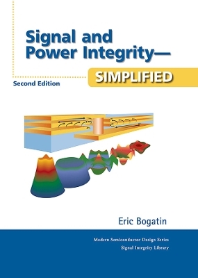
Signal and Power Integrity - Simplified
Pearson (Verlag)
978-0-13-234979-6 (ISBN)
- Titel erscheint in neuer Auflage
- Artikel merken
The #1 Practical Guide to Signal Integrity Design—Now Updated with Extensive New Coverage!
This book brings together up-to-the-minute techniques for finding, fixing, and avoiding signal integrity problems in your design. Drawing on his work teaching more than five thousand engineers, world-class signal and power integrity expert Eric Bogatin systematically reviews the root causes of all six families of signal integrity problems and shows how to design them out early in the design cycle. This edition’s extensive new content includes a brand-new chapter on S-parameters in signal integrity applications, and another on power integrity and power distribution network design—topics at the forefront of contemporary electronics design.
Coverage includes
A fully up-to-date introduction to signal integrity and physical design
How design and technology selection can make or break the performance of the power distribution network
Exploration of key concepts, such as plane impedance, spreading inductance, decoupling capacitors, and capacitor loop inductance
Practical techniques for analyzing resistance, capacitance, inductance, and impedance
Solving signal integrity problems via rules of thumb, analytic approximation, numerical simulation, and measurement
Understanding how interconnect physical design impacts signal integrity
Managing differential pairs and losses
Harnessing the full power of S-parameters in high-speed serial link applications
Ensuring power integrity throughout the entire power distribution path
Realistic design guidelines for improving signal integrity, and much more
Unlike books that concentrate on theoretical derivation and mathematical rigor, this book emphasizes intuitive understanding, practical tools, and engineering discipline. Designed for electronics industry professionals from beginners to experts it will be an invaluable resource for getting signal integrity designs right the first time, every time.
Eric Bogatin received his B.S. in physics from MIT in 1976 and his M.S. and Ph.D. in physics from the University of Arizona in Tucson in 1980. For more than thirty years he has been active in the fields of signal integrity and interconnect design. He worked in senior engineering and management roles at AT&T Bell Labs, Raychem Corp., Sun Microsystems, and Interconnect Devices Inc. Recognizing a need in the industry for quality technical training in signal integrity, he created Bogatin Enterprises, which has grown to be a world-leading provider of signal integrity training services. As a “Signal Integrity Evangelist,” Eric turns complexity into practical design principles, leveraging commercially available analysis techniques and measurement tools. Over the years, he has created a number of live classes and presented to more than five thousand engineers, worldwide. These include topics on transmission lines, differential pairs, switching noise, ground bounce, the power distribution network, and EMI. Some courses cover the use of TDR and VNA measurement techniques to characterize interconnects. In addition, Eric is a prolific author with more than three hundred publications, many posted on his web site, www.beTheSignal.com, for free download. He regularly presents at DesignCon, PCB West, Mentor User Group Meetings, and the IPC’s Designer Day annual event. In the past ten years, he has written regular monthly columns for Printed Circuit Design and Fabrication magazine, Semiconductor International, Electronic Packaging and Production, Altera Corporation, and Mentor Graphics Corporation. He is on the editorial board of Printed Circuit Design and Fabrication magazine and Microinterconnects Newsletter.
Preface to the Second Edition xv
Preface to the First Edition xvii
Acknowledgments xxiii
About the Author xxv
Chapter 1: Signal Integrity Is in Your Future 1
1.1 What Is Signal Integrity? 2
1.2 Signal Quality on a Single Net 5
1.3 Cross Talk 9
1.4 Rail-Collapse Noise 11
1.5 Electromagnetic Interference (EMI) 13
1.6 Two Important Signal Integrity Generalizations 16
1.7 Trends in Electronic Products 16
1.8 The Need for a New Design Methodology 22
1.9 A New Product Design Methodology 23
1.10 Simulations 24
1.11 Modeling and Models 27
1.12 Creating Circuit Models from Calculation 30
1.13 Three Types of Measurements 35
1.14 The Role of Measurements 38
1.15 The Bottom Line 39
Chapter 2: Time and Frequency Domains 43
2.1 The Time Domain 44
2.2 Sine Waves in the Frequency Domain 46
2.3 Shorter Time to a Solution in the Frequency Domain 48
2.4 Sine Wave Features 49
2.5 The Fourier Transform 51
2.6 The Spectrum of a Repetitive Signal 53
2.7 The Spectrum of an Ideal Square Wave 55
2.8 From the Frequency Domain to the Time Domain 57
2.9 Effect of Bandwidth on Rise Time 58
2.10 Bandwidth and Rise Time 62
2.11 What Does Significant Mean? 63
2.12 Bandwidth of Real Signals 67
2.13 Bandwidth and Clock Frequency 68
2.14 Bandwidth of a Measurement 70
2.15 Bandwidth of a Model 72
2.16 Bandwidth of an Interconnect 74
2.17 The Bottom Line 78
Chapter 3: Impedance and Electrical Models 81
3.1 Describing Signal-Integrity Solutions in Terms of Impedance 82
3.2 What Is Impedance? 84
3.3 Real Versus Ideal Circuit Elements 86
3.4 Impedance of an Ideal Resistor in the Time Domain 88
3.5 Impedance of an Ideal Capacitor in the Time Domain 89
3.6 Impedance of an Ideal Inductor in the Time Domain 92
3.7 Impedance in the Frequency Domain 94
3.8 Equivalent Electrical Circuit Models 99
3.9 Circuit Theory and SPICE 101
3.10 Introduction to Modeling 105
3.11 The Bottom Line 110
Chapter 4: The Physical Basis of Resistance 113
4.1 Translating Physical Design into Electrical Performance 114
4.2 The Only Good Approximation for the Resistance of Interconnects 115
4.3 Bulk Resistivity 118
4.4 Resistance per Length 119
4.5 Sheet Resistance 121
4.6 The Bottom Line 124
Chapter 5: The Physical Basis of Capacitance 127
5.1 Current Flow in Capacitors 128
5.2 The Capacitance of a Sphere 130
5.3 Parallel Plate Approximation 131
5.4 Dielectric Constant 133
5.5 Power and Ground Planes and Decoupling Capacitance 135
5.6 Capacitance per Length 138
5.7 2D Field Solvers 143
5.8 Effective Dielectric Constant 146
5.9 The Bottom Line 150
Chapter 6: The Physical Basis of Inductance 151
6.1 What Is Inductance? 151
6.2 Inductance Principle #1: There Are Circular Rings of Magnetic-Field Lines Around All Currents 152
6.3 Inductance Principle #2: Inductance Is the Number of Webers of Field Line Rings Around a Conductor per Amp of Current Through It 154
6.4 Self-Inductance and Mutual Inductance 156
6.5 Inductance Principle #3: When the Number of Field Line Rings Around a Conductor Changes, There Will Be a Voltage Induced Across the Ends of the Conductor 158
6.6 Partial Inductance 161
6.7 Effective, Total, or Net Inductance and Ground Bounce 167
6.8 Loop Self- and Mutual Inductance 173
6.9 The Power-Distribution Network (PDN) and Loop Inductance 178
6.10 Loop Inductance per Square of Planes 183
6.11 Loop Inductance of Planes and Via Contacts 184
6.12 Loop Inductance of Planes with a Field of Clearance Holes 187
6.13 Loop Mutual Inductance 188
6.14 Equivalent Inductance of Multiple Inductors 189
6.15 Summary of Inductance 191
6.16 Current Distributions and Skin Depth 193
6.17 High-Permeability Materials 202
6.18 Eddy Currents 204
6.19 The Bottom Line 206
Chapter 7: The Physical Basis of Transmission Lines 209
7.1 Forget the Word Ground 210
7.2 The Signal 211
7.3 Uniform Transmission Lines 212
7.4 The Speed of Electrons in Copper 214
7.5 The Speed of a Signal in a Transmission Line 215
7.6 Spatial Extent of the Leading Edge 219
7.7 “Be the Signal” 220
7.8 The Instantaneous Impedance of a Transmission Line 224
7.9 Characteristic Impedance and Controlled Impedance 227
7.10 Famous Characteristic Impedances 230
7.11 The Impedance of a Transmission Line 233
7.12 Driving a Transmission Line 238
7.13 Return Paths 241
7.14 When Return Paths Switch Reference Planes 244
7.15 A First-Order Model of a Transmission Line 257
7.16 Calculating Characteristic Impedance with Approximations 262
7.17 Calculating the Characteristic Impedance with a 2D Field Solver 265
7.18 An n-Section Lumped Circuit Model 270
7.19 Frequency Variation of the Characteristic Impedance 278
7.20 The Bottom Line 279
Chapter 8: Transmission Lines and Reflections 281
8.1 Reflections at Impedance Changes 282
8.2 Why Are There Reflections? 284
8.3 Reflections from Resistive Loads 288
8.4 Source Impedance 290
8.5 Bounce Diagrams 292
8.6 Simulating Reflected Waveforms 295
8.7 Measuring Reflections with a TDR 295
8.8 Transmission Lines and Unintentional Discontinuities 299
8.9 When to Terminate 301
8.10 The Most Common Termination Strategy for Point-to-Point Topology 304
8.11 Reflections from Short Series Transmission Lines 306
8.12 Reflections from Short-Stub Transmission Lines 309
8.13 Reflections from Capacitive End Terminations 311
8.14 Reflections from Capacitive Loads in the Middle of a Trace 314
8.15 Capacitive Delay Adders 317
8.16 Effects of Corners and Vias 319
8.17 Loaded Lines 325
8.18 Reflections from Inductive Discontinuities 327
8.19 Compensation 331
8.20 The Bottom Line 334
Chapter 9: Lossy Lines, Rise-Time Degradation, and Material Properties 337
9.1 Why Worry About Lossy Lines? 338
9.2 Losses in Transmission Lines 340
9.3 Sources of Loss: Conductor Resistance and Skin Depth 342
9.4 Sources of Loss: The Dielectric 346
9.5 Dissipation Factor 351
9.6 The Real Meaning of Dissipation Factor 354
9.7 Modeling Lossy Transmission Lines 360
9.8 Characteristic Impedance of a Lossy Transmission Line 367
9.9 Signal Velocity in a Lossy Transmission Line 369
9.10 Attenuation and the dB 371
9.11 Attenuation in Lossy Lines 376
9.12 Measured Properties of a Lossy Line in the Frequency Domain 385
9.13 The Bandwidth of an Interconnect 390
9.14 Time-Domain Behavior of Lossy Lines 397
9.15 Improving the Eye Diagram of a Transmission Line 400
9.16 Pre-emphasis and Equalization 402
9.17 The Bottom Line 403
Chapter 10: Cross Talk in Transmission Lines 405
10.1 Superposition 406
10.2 Origin of Coupling: Capacitance and Inductance 407
10.3 Cross Talk in Transmission Lines: NEXT and FEXT 409
10.4 Describing Cross Talk 411
10.5 The SPICE Capacitance Matrix 413
10.6 The Maxwell Capacitance Matrix and 2D Field Solvers 417
10.7 The Inductance Matrix 424
10.8 Cross Talk in Uniform Transmission Lines and Saturation Length 425
10.9 Capacitively Coupled Currents 431
10.10 Inductively Coupled Currents 435
10.11 Near-End Cross Talk 438
10.12 Far-End Cross Talk 441
10.13 Decreasing Far-End Cross Talk 448
10.14 Simulating Cross Talk 451
10.15 Guard Traces 457
10.16 Cross Talk and Dielectric Constant 464
10.17 Cross Talk and Timing 466
10.18 Switching Noise 469
10.19 Summary of Reducing Cross Talk 473
10.20 The Bottom Line 474
Chapter 11: Differential Pairs and Differential Impedance 475
11.1 Differential Signaling 476
11.2 A Differential Pair 480
11.3 Differential Impedance with No Coupling 482
11.4 The Impact from Coupling 486
11.5 Calculating Differential Impedance 493
11.6 The Return-Current Distribution in a Differential Pair 496
11.7 Odd and Even Modes 502
11.8 Differential Impedance and Odd-Mode Impedance 507
11.9 Common Impedance and Even-Mode Impedance 508
11.10 Differential and Common Signals and Odd- and Even-Mode Voltage Components 511
11.11 Velocity of Each Mode and Far-End Cross Talk 513
11.12 Ideal Coupled Transmission-Line Model or an Ideal Differential Pair 519
11.13 Measuring Even- and Odd-Mode Impedance 520
11.14 Terminating Differential and Common Signals 522
11.15 Conversion of Differential to Common Signals 529
11.16 EMI and Common Signals 534
11.17 Cross Talk in Differential Pairs 539
11.18 Crossing a Gap in the Return Path 542
11.19 To Tightly Couple or Not to Tightly Couple 544
11.20 Calculating Odd and Even Modes from Capacitance- and Inductance-Matrix Elements 546
11.21 The Characteristic Impedance Matrix 550
11.22 The Bottom Line 553
Chapter 12: S-Parameters for Signal Integrity Applications 555
12.1 S-Parameters, the New Universal Metric 555
12.2 What Are S-Parameters? 557
12.3 Basic S-Parameter Formalism 559
12.4 S-Parameter Matrix Elements 562
12.5 Simulating Return and Insertion Loss 567
12.6 A Transparent Interconnect 570
12.7 Changing the Port Impedance 573
12.8 The Phase of S21 for a Uniform 50-Ohm Transmission Line 574
12.9 The Magnitude of S21 for a Uniform Transmission Line 577
12.10 Coupling to Other Transmission Lines 582
12.11 Insertion Loss for Non-50-Ohm Transmission Lines 589
12.12 Data-Mining S-Parameters 594
12.13 Single-Ended and Differential S-Parameters 596
12.14 Differential Insertion Loss 601
12.15 The Mode Conversion Terms 605
12.16 Converting to Mixed-Mode S-Parameters 607
12.17 Time and Frequency Domains 609
12.18 The Bottom Line 613
Chapter 13: The Power Distribution Network (PDN) 615
13.1 The Problem 615
13.2 The Root Cause 618
13.3 The Most Important Design Guidelines for the PDN 620
13.4 Establishing the Target Impedance Is Hard 621
13.5 Every Product Has a Unique PDN Requirement 629
13.6 Engineering the PDN 631
13.7 The VRM 633
13.8 Simulating Impedance with SPICE 635
13.9 On-die Capacitance 637
13.10 The Package Barrier 639
13.11 The PDN with No Decoupling Capacitors 644
13.12 The MLCC Capacitor 646
13.13 The Equivalent Series Inductance 650
13.14 Approximating Loop Inductance 652
13.15 Optimizing the Mounting of Capacitors 661
13.16 Combining Capacitors in Parallel 667
13.17 Engineering a Reduced Parallel Resonant Peak by Adding More Capacitors 673
13.18 Selecting Capacitor Values 675
13.19 Estimating the Number of Capacitors Needed 681
13.20 How Much Does a nH Cost? 683
13.21 Quantity or Specific Values? 687
13.22 Sculpting the Impedance Profiles: The Frequency Domain Target Impedance (FDTI) Method 692
13.23 When Every pH Counts 699
13.24 Location, Location, Location 703
13.25 When Spreading Inductance Is the Limitation 707
13.26 The Chip View 710
13.27 Bringing It All Together 713
13.28 The Bottom Line 717
Appendix A: 100 General Design Guidelines to Minimize Signal-Integrity Problems 719
Appendix B: 100 Collected Rules of Thumb to Help Estimate Signal-Integrity Effects 727
Appendix C: Selected References 739
Index 741
| Erscheint lt. Verlag | 30.7.2009 |
|---|---|
| Reihe/Serie | Signal Integrity Library |
| Sprache | englisch |
| Maße | 180 x 235 mm |
| Gewicht | 1140 g |
| Themenwelt | Technik ► Elektrotechnik / Energietechnik |
| ISBN-10 | 0-13-234979-5 / 0132349795 |
| ISBN-13 | 978-0-13-234979-6 / 9780132349796 |
| Zustand | Neuware |
| Informationen gemäß Produktsicherheitsverordnung (GPSR) | |
| Haben Sie eine Frage zum Produkt? |
aus dem Bereich


