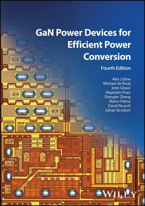
GaN Power Devices for Efficient Power Conversion (eBook)
1027 Seiten
Wiley (Verlag)
978-1-394-28697-3 (ISBN)
An up-to-date and concise review of GaN transistor design and applications
In the newly revised fourth edition of GaN Power Devices for Efficient Power Conversion, a team of distinguished researchers and practicing engineers deliver a concise and effective new guide to designing small, energy-efficient, and inexpensive products with GaN transistors. This new edition covers all relevant new GaN technology advancements, allowing students and practicing engineers to get, and stay ahead of, the curve with GaN device and circuit technology.
You'll explore applications including DC to DC converters, solar inverters, motor drive controllers, satellite electronics, and LiDAR devices. The 4th edition offers critical updates for space applications, vertical GaN, and driving transistors and integrated circuits. New chapters on reliability testing advancements, device wear out mechanisms, thermal management, and the latest developments in monolithic integration round out the book.
Readers will also find:
- The latest updates on significant technology improvements, like integrated circuits, reliability studies, and new applications
- Comprehensive explorations of integrated circuit construction, characteristics, reliability results, and applications
- Practical discussions of specific circuit designs, layout, and thermal dissipation when designing power conversion systems
- Chapters written by practicing expert leaders in the power semiconductor field and industry pioneers
Perfect for practicing power conversion engineers, GaN Power Devices for Efficient Power Conversion will also benefit electrical engineering students and device scientists in the field of power electronics.
Alex Lidow is the CEO and Co-founder of Efficient Power Conversion.
Michael de Rooij is Vice President of Applications Engineering at Efficient Power Conversion.
John Glaser is Director of Applications at Efficient Power Conversion.
Alejandro Pozo is a Senior Applications Engineer at Efficient Power Conversion.
Shengke Zhang is Vice President of Product Reliability at Efficient Power Conversion.
Marco Palma is a Senior FAE Manager based in Europe.
David Reusch is a Systems Engineer, Kilby Labs, Texas Instruments, USA.
Johan Strydom is Advanced Development Manager, Kilby Labs, Texas Instruments, USA.
1
GaN Technology Overview
1.1 Silicon Power MOSFETs: 1976–2010
For over three decades, power management efficiency and cost have improved steadily as innovations in power Metal Oxide Silicon Field‐Effect Transistor (MOSFET) structures, technology, and circuit topologies have kept pace with the growing need for electrical power in our daily lives. In the new millennium, however, the rate of improvement has slowed as the silicon power MOSFET asymptotically approaches its theoretical bounds.
Power MOSFETs first appeared in 1976 as alternatives to bipolar transistors. These majority‐carrier devices were faster, more rugged, and had higher current gain than their minority‐carrier counterparts (for a discussion of basic semiconductor physics, a good reference is [1]). As a result, switching power conversion became a commercial reality. Among the earliest high‐volume consumers of power MOSFETs were AC–DC switching power supplies for early desktop computers, followed by variable‐speed motor drives, fluorescent lights, DC–DC converters, and thousands of other applications that populate our daily lives.
One of the first power MOSFETs was the IRF100 from International Rectifier Corporation, introduced in November 1978. It boasted a 100 V drain–source breakdown voltage and a 0.1 Ω on‐resistance (R DS(on)), the benchmark of the era. With a die size over 40 mm2 and a $34 price tag, this product was not destined to supplant the venerable bipolar transistor immediately. Since then, several manufacturers have developed many generations of power MOSFETs. Benchmarks have been set, and subsequently surpassed, each year for 40‐plus years. As of the date of this writing, the 100 V benchmark arguably is held by Infineon with the ISC022N10NM6. In comparison with the IRF100 MOSFET’s resistivity figure of merit (4 Ω – mm2), the ISC022N10NM6 has a figure of merit of 0.022 Ω – mm2. That is almost at the theoretical limit for a silicon device [2].
There are still improvements to be made in power MOSFETs. For example, super‐junction devices and IGBTs have achieved conductivity improvements beyond the theoretical limits of a simple vertical, majority‐carrier MOSFET. These innovations may still continue for quite some time and certainly will be able to leverage the low‐cost structure of the power MOSFET and the know‐how of a well‐educated base of designers who, after many years, have learned to squeeze every ounce of performance out of their power conversion circuits and systems.
1.2 The GaN Journey Begins
Gallium nitride (GaN) is called a wide bandgap (WBG) semiconductor due to the relatively large bonding energy of the atomic components in its crystal structure. Silicon carbide (SiC) is the other most common WBG semiconductor. GaN HEMT (High Electron Mobility Transistors) devices first appeared in about 2004 with depletion‐mode radio frequency (RF) transistors made by Eudyna Corporation in Japan. Using GaN‐on‐silicon carbide substrates, Eudyna successfully produced transistors designed for the RF market [3]. The HEMT structure was based on the phenomenon first described in 1975 by Mimura et al. [4] and in 1991 by Khan et al. [5], which demonstrated the unusually high electron mobility described as a two‐dimensional electron gas (2DEG) near the interface between an aluminum gallium nitride (AlGaN) and GaN heterostructure interface. Adapting this phenomenon to gallium nitride grown on silicon carbide, Eudyna was able to produce benchmark power gain in the multi‐gigahertz frequency range. In 2005, Nitronex Corporation introduced the first depletion‐mode RF HEMT device made with GaN grown on silicon wafers using their SIGANTIC® technology.
GaN RF transistors have continued to make inroads in RF applications as several other companies have entered the market. Acceptance outside of this application, however, has been limited by device cost as well as the inconvenience of depletion‐mode operation (normally conducting and requires a negative voltage on the gate to turn the device off).
In June 2009, Efficient Power Conversion Corporation (EPC) introduced the first enhancement‐mode GaN on silicon (eGaN®) field‐effect transistors (FETs) designed specifically as power MOSFET replacements (since eGaN FETs do not require a negative voltage to be turned off). At the outset, these products were produced in high volume at low cost by using standard silicon manufacturing technology and facilities. Since then, Texas Instruments, VisIC, Cambridge GaN Devices, ST Microelectronics, Transphorm (now part of Renesas), GaN Systems (now part of Infineon), Panasonic, TSMC, Navitas, Innoscience, and Infineon, among others, have announced their intention to manufacture GaN transistors for the power conversion market.
The basic requirements for semiconductors used in power conversion are efficiency, reliability, controllability, and cost effectiveness. Without these attributes, a new device structure would not be economically viable. There have been many new structures and materials considered as a successor to silicon; some have been economic successes, others have seen limited or niche acceptance. In the next section, we will look at the comparison between silicon, SiC, and GaN as platform candidates to dominate the next generation of power transistors.
1.3 GaN and SiC Compared with Silicon
Silicon has been a dominant material for power management since the late 1950s. The advantages silicon had over earlier semiconductors, such as germanium or selenium, could be expressed in four key categories:
- silicon enabled new applications not possible with earlier materials
- silicon proved more reliable
- silicon was easier to use in many ways
- silicon devices cost less.
All of these advantages stemmed from the basic physical properties of silicon combined with a huge investment in manufacturing infrastructure and engineering. Let us look at some of those basic properties and compare them with other successor candidates. Table 1.1 identifies five key electrical properties of three semiconductor materials contending for the power management market.
Table 1.1 Material properties of GaN, 4H‐SiC, and Si [6].
| Parameter | Silicon | GaN | SiC |
|---|
| Band gap (E g) | eV | 1.12 | 3.39 | 3.26 |
| Critical field (E crit) | MV/cm | 0.23 | 3.3 | 2.2 |
| Electron mobility (μ n) | cm2/V·s | 1400 | 1500 | 950 |
| Permittivity (ε r) | 11.8 | 9 | 9.7 |
| Thermal conductivity (λ) | W/cm·K | 1.5 | 1.3 | 3.8 |
One way of translating these basic crystal parameters into a comparison of device performance is to calculate the best theoretical performance achievable for each of the three candidates. For power devices, there are many characteristics that matter in the variety of power conversion systems available today. Five of the most important are conduction efficiency (on‐resistance), breakdown voltage, size, switching efficiency, and cost.
In the next section, the first four of the material characteristics in Table 1.1 will be reviewed, leading to the conclusion that both SiC [7] and GaN are capable of producing devices with superior on‐resistance, breakdown voltage, and a smaller‐sized transistor compared to silicon (Si). In Chapter 2, how these material characteristics translate into superior switching efficiency for a GaN transistor will be explored, and in Chapter 16, how a GaN transistor can also be produced at a lower cost than a silicon MOSFET of equivalent performance will be addressed.
1.3.1 Band Gap (Eg)
The band gap of a semiconductor is related to the strength of the chemical bonds between the atoms in the lattice. These stronger bonds mean that it is harder for an electron to jump from one site to the next. Among the many consequences are lower intrinsic leakage currents and higher operating temperatures for higher band gap semiconductors. Based on the data in Table 1.1, both GaN and SiC have higher band gaps than silicon.
1.3.2 Critical Field (Ecrit)
The stronger chemical bonds that cause the wider band gap also result in a higher critical electric field needed to initiate impact ionization, which results in avalanche breakdown. The voltage at which a device breaks down can be approximated with the formula:
The breakdown voltage of a device (V BR), therefore, is proportional to the width of the drift region (w drift). In the case of SiC and GaN, the drift region can be 10 times smaller than in silicon for the same breakdown voltage. In order to support this electric field, there need...
| Erscheint lt. Verlag | 31.12.2024 |
|---|---|
| Sprache | englisch |
| Themenwelt | Technik ► Elektrotechnik / Energietechnik |
| Schlagworte | Gallium nitride • gallium nitride integrated circuits • Gallium nitride transistors • GaN applications including dc-dc power conversion • GaN Reliability • Lidar • motor drive contollers • Power devices • Power Integrated Circuits • Power semiconductors • Satellites |
| ISBN-10 | 1-394-28697-X / 139428697X |
| ISBN-13 | 978-1-394-28697-3 / 9781394286973 |
| Informationen gemäß Produktsicherheitsverordnung (GPSR) | |
| Haben Sie eine Frage zum Produkt? |
Größe: 40,1 MB
Kopierschutz: Adobe-DRM
Adobe-DRM ist ein Kopierschutz, der das eBook vor Mißbrauch schützen soll. Dabei wird das eBook bereits beim Download auf Ihre persönliche Adobe-ID autorisiert. Lesen können Sie das eBook dann nur auf den Geräten, welche ebenfalls auf Ihre Adobe-ID registriert sind.
Details zum Adobe-DRM
Dateiformat: EPUB (Electronic Publication)
EPUB ist ein offener Standard für eBooks und eignet sich besonders zur Darstellung von Belletristik und Sachbüchern. Der Fließtext wird dynamisch an die Display- und Schriftgröße angepasst. Auch für mobile Lesegeräte ist EPUB daher gut geeignet.
Systemvoraussetzungen:
PC/Mac: Mit einem PC oder Mac können Sie dieses eBook lesen. Sie benötigen eine
eReader: Dieses eBook kann mit (fast) allen eBook-Readern gelesen werden. Mit dem amazon-Kindle ist es aber nicht kompatibel.
Smartphone/Tablet: Egal ob Apple oder Android, dieses eBook können Sie lesen. Sie benötigen eine
Geräteliste und zusätzliche Hinweise
Buying eBooks from abroad
For tax law reasons we can sell eBooks just within Germany and Switzerland. Regrettably we cannot fulfill eBook-orders from other countries.
aus dem Bereich


