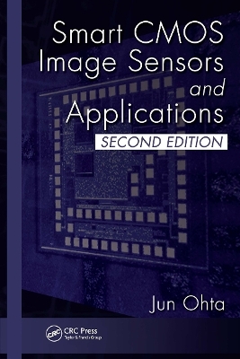
Smart CMOS Image Sensors and Applications
CRC Press (Verlag)
978-1-032-65236-8 (ISBN)
Revised and expanded for this new edition, Smart CMOS Image Sensors and Applications, Second Edition is the only book available devoted to smart CMOS image sensors and applications. The book describes the fundamentals of CMOS image sensors and optoelectronic device physics, and introduces typical CMOS image sensor structures, such as the active pixel sensor (APS). Also included are the functions and materials of smart CMOS image sensors and present examples of smart imaging. Various applications of smart CMOS image sensors are also discussed. Several appendices supply a range of information on constants, illuminance, MOSFET characteristics, and optical resolution. Expansion of smart materials, smart imaging and applications, including biotechnology and optical wireless communication, are included.
Features
• Covers the fundamentals and applications including smart materials, smart imaging, and various applications
• Includes comprehensive references
• Discusses a wide variety of applications of smart CMOS image sensors including biotechnology and optical wireless communication
• Revised and expanded to include the state of the art of smart image sensors
Jun Ohta received the B.E., M.E., and Dr. Eng. degrees in applied physics, all from the University of Tokyo, Japan, in 1981, 1983, and 1992, respectively. In 1983, he joined Mitsubishi Electric Corporation, Hyogo, Japan. From 1992 to 1993, he was a visiting scientist in Optoelectronics Computing Systems Center, University of Colorado at Boulder. In 1998, he joined Graduate School of Materials Science, Nara Institute of Science and Technology (NAIST), Nara, Japan as Associate Professor. He was appointed as Professor in 2004. His current research interests are smart CMOS image sensors for biomedical applications and retinal prosthetic devices. He serves as the Distinguished Lecturer of IEEE Solid-State Circuits Society, a section editor of IET Journal of Engineering, an associate editor of IEEE Trans. Biomedical Circuits and Systems, an editor of Japanese Journal of Applied Physic, etc. He also served as technical program committee member of IEEE ISSCC, Symposium on VLSI Circuits, IEEE BioCAS 2018, etc. He organized the IEEE BioCAS 2019 at Nara as one of the general co-chairs. He is a senior member of both IEEE and the IEE Japan, and a fellow member of both the JSAP and the ITE Japan.
1 Introduction. A general overview. 1.2 Brief history of CMOS image sensors . 1.3 Brief history of smart CMOS image sensors. 1.4 Organization of the book. 2 Fundamentals of CMOS image sensors. 2.1 Introduction. 2.2 Fundamentals of photo detection. 2.2.1 Absorption coefficient. 2.2.2 Behavior of minority carriers. 2.2.3 Sensitivity and quantum efficiency. 2.3 Photodetectors for smart CMOS image sensors. 2.3.1 pn-junction photodiode. 2.3.2 Photogate. 2.3.3 Phototransistor. 2.3.4 Avalanche photodiode. 2.3.5 Photoconductive detector. 2.4 Accumulation mode in PDs.. 2.4.1 Potential change in accumulation mode. 2.4.2 Potential description. 2.4.3 Behavior of photo-generated carriers in PD. 2.5 Basic pixel structures. 2.5.1 Passive pixel sensor. 2.5.2 Active pixel sensor,3T-APS. 2.5.3 Active pixel sensor,4T-APS. 2.6 Sensor peripherals. 2.6.1 Addressing. 2.6.2 Readout circuits. 2.6.3 Analog-to-digital converters. 2.7 Basic sensor characteristics. 2.7.1 Noise. 2.7.2 Dynamic range. 2.7.3 Speed. 2.8 Color. 2.9 Pixel sharing. 2.10 Comparison between pixel architecture. 2.11 Comparison with CCDs. 3 Smart functions and materials. 3.1 Introduction 3.2 Pixel structure. 3.2.1 Current mode. 3.2.2 Log sensor. 3.3 Analog operation. 3.3.1 Winner-take-all. 3.3.2 Projection. 3.3.3 Resistive network. 3.4 Pulse modulation. 3.4.1 Pulse width modulation. 3.4.2 Pulse frequency modulation. 3.5 Digital processing. 3.6 Materials other than silicon. 3.6.1 Silicon-on-insulator. 3.6.2 Extending the detection wavelength. 3.7 Structures other than standard CMOS technologies. 3.7.1 3D integration. 3.7.2 Integration with light emitters. 3.7.3 Color realization using nonstandard structures. 4 Smart imaging. 4.1 Introduction. 4.2 Low light imaging. 4.2.2 PFM for lowlight imaging. 4.2.3 Differential APS. 4.2.4 Geiger mode APD for a smart CMOS image sensor. 4.3 High speed. 4.3.1 Global shutter. 4.4 Wide dynamic range. 4.4.1 Principle of wide dynamic range. 4.4.2 Dual sensitivity. 4.4.3 Nonlinear response. 4.4.4 Multiple sampling. 4.4.5 Saturation detection. 4.4.6 Diffusive brightness. 4.5 Demodulation. 4.5.1 Principles of demodulation. 4.5.2 Correlation. 4.5.3 Method of two accumulation regions. 4.6 Three-dimensional rangefinder. 4.6.1 Time of flight. 4.6.2 Triangulation. 4.6.3 Depth key. 4.7 Target tracking. 4.7.1 Maximum detection for target tracking. 4.7.2 Projection for target tracking. 4.7.3 Resistive network and other analog processing for target. Tracking. 4.7.4 Digital processing for target tracking. 4.8 Dedicated arrangement of pixel and optics. 4.8.1 Non-orthogonal arrangement. 4.8.2 Dedicated optics. 4.8.3 Light field detection. 4.9 Polarization detection. 5 Applications. 5.1 Introduction. 5.2 Information and communication applications. 5.2.1 Optical ID tag. 5.2.2 Optical wireless communication. 5.3 Biotechnology applications. 5.3.1 Smart CMOS image sensor with multi-modal functions. 5.3.2 Smart CMOS image sensor with ISFET. 5.3.3 Potential imaging combining MEMS technology. 5.3.4 Smart CMOS sensor for optical and electrochemical imaging. 5.3.5 Fluorescence detection. 5.4 Medical applications. 5.4.1 Capsule endoscope. 5.4.2 Retinal prosthesis. A Tables of constants. B Illuminance. C Human eye and CMOS image sensors. D Fundamental characteristics of MOS capacitors. E Fundamental characteristics of MOSFET. F Optical format and resolution. References. Index
| Erscheinungsdatum | 23.08.2024 |
|---|---|
| Reihe/Serie | Optical Science and Engineering |
| Verlagsort | London |
| Sprache | englisch |
| Maße | 156 x 234 mm |
| Gewicht | 570 g |
| Themenwelt | Technik ► Maschinenbau |
| Technik ► Nachrichtentechnik | |
| ISBN-10 | 1-032-65236-5 / 1032652365 |
| ISBN-13 | 978-1-032-65236-8 / 9781032652368 |
| Zustand | Neuware |
| Informationen gemäß Produktsicherheitsverordnung (GPSR) | |
| Haben Sie eine Frage zum Produkt? |
aus dem Bereich


