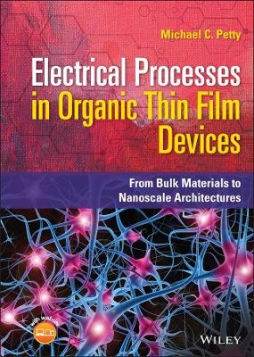
Electrical Processes in Organic Thin Film Devices
John Wiley & Sons Inc (Verlag)
978-1-119-63127-9 (ISBN)
In Electrical Processes in Organic Thin Film Devices: From Bulk Materials to Nanoscale Architectures, distinguished researcher Michael C. Petty delivers an in-depth treatment of the electrical behaviour of organic electronic devices focused on first principles. The author describes the fundamental electrical behaviour of various device architectures and offers an introduction to the physical processes that play a role in the electrical conductivity of organic materials.
Beginning with band theory, the text moves on to address the effects of thin film device architectures and nanostructures. The book discusses the applications to devices currently in the marketplace, like displays, as well as those under development (transistors, solar cells, and memories).
Electrical Processes in Organic Thin Film Devices also describes emerging organic thin film architectures and explores the potential for single molecule electronics and biologically inspired devices. Finally, the book also includes:
A detailed introduction to electronic and vibrational states in organic solids, including classical band theory, disordered semiconductors, and lattice vibrations
Comprehensive explorations of electrical conductivity, including electronic and ionic processes, carrier drift, diffusion, the Boltzmann Transport Equation, excess carriers, recombination, doping, and superconductivity
An overview of important electro-active organic materials, like molecular crystals, charge-transfer complexes, conductive polymers, carbon nanotubes, and graphene
Practical considerations of defects and nanoscale phenomena, including transport processes in low-dimensional systems, surfaces and interface states
In-depth examinations of metal contacts, including ohmic contacts, the Schottky Barrier, and metal/molecule contacts
A systematic guide to the operating principles of metal/insulator/semiconductor structures and the field effect
A set of problems (with solutions on-line) for each chapter of the book
Perfect for electronics developers and researchers in both industry and academia who study and work with molecular and nanoscale electronics, Electrical Processes in Organic Thin Film Devices also deserves a place in the libraries of undergraduate and postgraduate students in courses on molecular electronics, organic electronics, and plastic electronics.
Michael C. Petty is Professor Emeritus in the Department of Engineering at the University of Durham in the United Kingdom. He is Past President of the International Society for Molecular Electronics and Biocomputing and a previous Chairman of the School of Engineering at Durham University. He has published extensively in the areas of organic electronics and molecular electronics.
Chapter 1 – Electronic and Vibrational States in Organic Solids
1.1 Introduction
1.2 Band Theory for Inorganic Single Crystals
1.2.1 Schrödinger Wave Equation
1.2.2 Density of Electron States
1.2.3 Occupation of Energy States
1.2.4 Conductors, Semiconductors and Insulators
1.2.5 Electrons and Holes
1.2.6 Doping
1.3 Lattice Vibrations
1.4 Amorphous Inorganic Semiconductors
1.5 Organic Semiconductors
1.5.1 Electronic Orbitals and Bands in Important Organic Compounds
1.5.2 Molecular Crystals
1.5.3 Polymers
1.5.4 Charge-transfer Complexes
1.5.5 Graphene
1.5.6 Fullerenes and Carbon Nanotubes
1.5.7 Doping of Organic Semiconductors
Problems
References
Further Reading
Chapter 2 – Electrical Conductivity: Fundamental Principles
2.1 Introduction
2.2 Classical Model
2.3 Boltzmann Transport Equation
2.4 Ohm’s Law
2.5 Charge Carrier Mobility
2.6 Equilibrium Carrier Statistics
2.6.1 Intrinsic Conduction
2.6.2 Carrier Generation and Recombination
2.6.3 Extrinsic Conduction
2.6.4 Fermi Level Position
2.6.5 Meyer-Neldel Rule
2.7 Excess Carriers
2.7.1 Quasi-Fermi Level
2.7.2 Diffusion and Drift
2.7.3 Gradients in the Quasi-Fermi Levels
2.7.4 Carrier Lifetime
2.8 Superconductivity
Problems
References
Further Reading
Chapter 3 – Defects and Nanoscale Phenomena
3.1 Introduction
3.2 Material Purity
3.3 Point and Line Defects
3.4 Traps and Recombination Centres
3.4.1 Direct Recombination
3.4.2 Recombination via Traps
3.5 Grain Boundaries and Surfaces
3.5.1 Interface States
3.6 Polymer Defects
3.6.1 Solitons
3.6.2 Polarons and Bipolarons
3.7 Disordered Semiconductors
3.8 Electron Transport in Low Dimensional Systems
3.8.1 Two-dimensional Transport
3.8.2 One-dimensional Transport
3.8.3 Zero-dimensional Transport
3.9 Nanosystems
3.9.1 Scaling Laws
3.9.2 Interatomic Forces
Problems
References
Further Reading
Chapter 4 – Electrical Contacts: Ohmic and Rectifying Behaviour
4.1 Introduction
4.2 Practical Considerations
4.3 Neutral, Ohmic and Blocking Contacts
4.4 Schottky Barrier
4.4.1 Barrier Formation
4.4.2 Image Force
4.4.3 Current versus Voltage Behaviour
4.4.4 Effect of an Interfacial Layer
4.4.5 Organic Schottky Diodes
4.5 Molecular Devices
4.5.1 Metal/Molecule Contacts
4.5.2 Break Junctions
4.5.3 Molecular Rectifying Diodes
4.5.4 Molecular Resonant Tunnelling Devices
Problems
References
Further Reading
Chapter 5 – Metal/Insulator/Semiconductor Devices: The Field Effect
5.1 Introduction
5.2 Ideal MIS device
5.3 Departures from Ideality
5.3.1 Insulator Charge and Work Function Differences
5.3.2 Interface Traps
5.4 Organic MIS Devices
5.4.1 Inorganic Semiconductor/Organic Insulator Structures
5.4.2 Organic Semiconductor Structures
Problems
References
Further Reading
Chapter 6 – DC Conductivity
6.1 Introduction
6.2 Electronic versus Ionic Conductivity
6.3 Quantum Mechanical Tunnelling
6.4 Variable Range Hopping
6.5 Fluctuation-induced Tunnelling
6.6 Space Charge Injection
6.6.1 Effect of Traps
6.6.2 Two-carrier Injection
6.7 Schottky, Fowler-Nordheim and Poole-Frenkel Effects
6.8 Electrical Breakdown
6.8.1 Intrinsic Breakdown
6.8.2 Electromechanical Breakdown
6.8.3 Thermal Runaway
6.8.4 Contact Instability
6.8.5 Other Effects
6.9 Electromigration
6.10 Measurement of Trapping Parameters
6.10.1 Thermally Stimulated Conductivity
6.10.2 Capacitance Spectroscopy
Problems
References
Further Reading
Chapter 7 – Polarization and AC Conductivity
7.1 Introduction
7.2 Polarization
7.2.1 Dipole Creation
7.2.2 Permanent Polarization
7.2.3 Piezoelectricity, Pyroelectricity and Ferroelectricity
7.3 Conductivity at High Frequencies
7.3.1 Displacement Current
7.3.2 Frequency-dependent Permittivity
7.3.3 AC Conductivity
7.4 Impedance Spectroscopy
7.5 AC Electrical Measurements
7.5.1 Lock-in Amplifier
7.5.2 Scanning Microscopy
7.6 Electrical Noise
Problems
References
Further Reading
Chapter 8 – Organic Field Effect Transistors
8.1 Introduction
8.2 Physics of Operation
8.3 Transistor Fabrication
8.4 Practical Device Behaviour
8.4.1 Contact Resistance
8.4.2 Material Morphology and Traps
8.4.3 Short Channel Effects
8.4.4 Organic Semiconductors
8.4.5 Gate Dielectric
8.5 Organic Integrated Circuits
8.6 Nanotube and Graphene FETs
8.7 Single-electron Transistors
8.8 Transistor-based Chemical Sensors
8.8.1 Ion-sensitive FETs
8.8.2 Charge-flow Transistor
Problems
References
Further Reading
Chapter 9 – Electronic Memory
9.1 Introduction
9.2 Memory Types
9.3 Resistive Memory
9.4 Organic Flash Memory
9.5 Ferroelectric RAMs
9.6 Spintronics
9.7 Molecular Memories
Problems
References
Further Reading
Chapter 10 – Light-emitting Devices
10.1 Introduction
10.2 Light Emission Processes
10.3 Operating Principles
10.4 Colour Measurement
10.5 Photometric Units
10.6 OLED Efficiency
10.7 Device Architectures
10.7.1 Top- and Bottom-emitting OLEDs
10.7.2 Electrodes
10.7.3 Hole- and Electron-transport Layers
10.7.4 Triplet Management
10.7.5 Blended-layer and Molecularly-engineered Devices
10.8 Increasing the Light Output
10.8.1 Efficiency Losses
10.8.2 Microlenses and Shaped Substrates
10.8.3 Microcavities
10.8.4 Device Degradation
10.9 Full-colour Displays
10.10 Organic Semiconductor Lasers
10.11 OLED Lighting
10.12 Light-emitting Electrochemical Cells
10.13 Light-emitting Transistors
Problems
References
Further Reading
Chapter 11 – Photoconductive and Photovoltaic Devices
11.1 Introduction
11.2 Photoconductivity
11.2.1 Optical Absorption
11.2.2 Carrier Lifetime
11.2.3 Photosenstivity
11.3 Xerography
11.4 Photovoltaic Principles
11.4.1 Electrical Characteristics
11.4.2 Efficiency
11.5 Organic Solar Cells
11.5.1 Carrier Collection
11.5.2 Bulk Heterojunction Solar Cells
11.5.3 Electrodes and Device Architectures
11.5.4 Tandem Cells
11.5.5 Upconversion
11.5.6 Device Degradation
11.6 Dye-sensitized Solar Cells
11.7 Hybrid Solar Cells
11.7.1 Polymer-Metal Oxide Devices
11.7.2 Inorganic Semiconductor-Polymer Hole-transporter Cells
11.7.3 Perovskite Solar Cells
11.8 Luminescent Solar Concentrator
11.9 Organic Photodiodes and Phototransistors
Problems
References
Further Reading
Chapter 12 – Emerging Devices and Systems
12.1 Introduction
12.2 Molecular Logic Circuits
12.3 Inspiration from the Natural World
12.3.1 Amino Acids, Peptides and Proteins
12.3.2 Nucleotides, DNA and RNA
12.3.3 ATP, ADP
12.3.4 The Biological Membrane and Ion Transport
12.3.5 Electron Transport
12.3.6 Neurons
12.4 Computing Strategies
12.4.1 Von Neumann Computer
12.4.2 Biological Information Processing
12.4.3 Artificial Neural Networks
12.4.4 Organic Neuromorphic Devices
12.4.5 DNA and Microtubule Electronics
12.4.6 Quantum Computing
12.4.7 Evolvable Electronics
12.5 Fault Tolerance and Self Repair
12.6 Bacteriorhodopsin – A Light-driven Proton Pump
12.7 Photosynthesis and Artificial Molecular Architectures
12.8 Bio-chemical Sensors
12.8.1 Biocatalytic Sensors
12.8.2 Bioaffinity Sensors
12.9 Electronic Olfaction and Gustation
Problems
References
Further Reading
| Erscheinungsdatum | 18.02.2022 |
|---|---|
| Verlagsort | New York |
| Sprache | englisch |
| Maße | 178 x 254 mm |
| Gewicht | 680 g |
| Themenwelt | Technik ► Elektrotechnik / Energietechnik |
| Technik ► Maschinenbau | |
| ISBN-10 | 1-119-63127-0 / 1119631270 |
| ISBN-13 | 978-1-119-63127-9 / 9781119631279 |
| Zustand | Neuware |
| Informationen gemäß Produktsicherheitsverordnung (GPSR) | |
| Haben Sie eine Frage zum Produkt? |
aus dem Bereich


