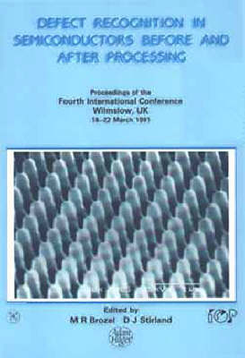
Defect Recognition in Semiconductors Before and After Processing, Proceedings of the Fourth INT Conference held 18-22 March 1991
Institute of Physics Publishing (Verlag)
978-0-7503-0188-6 (ISBN)
- Titel ist leider vergriffen;
keine Neuauflage - Artikel merken
the major interests of semiconductor device manufacturers is yield. In many cases this critical parameter can be directly related to material uniformity. Uniformity is important at all stages of processing, from substrate procurement to device fabrication. Mapping of non-uniformities in semiconductors has resulted in the development of specialized techniques - the subjects of the DRIP conference series. Like its predecessors, the fourth conference in the DRIP series brought together a group of international experts in uniformity assessment and mapping for a successful exchange of information and ideas. The central theme of the meeting reflected the current need to recognize defects in semiconductor materials during the large scale production of devices ranging from light emitting diodes to microwave integrated circuits. Topics such as the quality of epitaxial growth, yields of integrated circuits and the imaging of non-uniformities were discussed in detail. The refereed proceedings of this important, topical conference have been brought together in this volume providing a thorough account of the latest developments in this exciting area of semiconductor research. The papers presented here are reprinted from Semiconductor Science and Technology (1992, Volume 7, Number 1A), an Institute of Physics journal.
Scanned photoluminescence of semiconductors (H J Hovel). Non-destructive, whole wafer assessment of optoelectronic epitaxial materials (C J Miner). Low-temperature photoluminescence topography of MOCVD-grown InGaP, AlGaAs and AlGaAs/GaAs single quantum wells (K H Bachem and W Jantz et al). Scanned photoluminescence with high spatial resolution in semi-insulating GaAs and InP: aspects of surface passivation and photodegradation (G E Carver). Spatial variations of photoluminescence line broadening around oval defects in GaAs/AlGaAs multiple quantum wells (J E M Haverkort and J H Wolter et al). Makyoh topography: comparison with x-ray topography (K Kugimiya). Recovery of damaged GaAs diodes by minority carrier injection (K Yamada and K Wada). The scanning infrared microscope (SIRM) and its application to bulk GaAs and Si: a review (G R Booker et al). X-ray topography and diffractometry of strained layer heteroepitaxial structures (S J Barnett et al). Non-contact observations of photoconductivity decay and carrier lifetime measurements in epitaxial silicon wafers (Y Ogita). Non-contact mapping of heavy metal contamination for silicon IC fabrication (J Lagowski and W Henley et al). Defects in and device properties of semi-insulating GaAs (O Oda and M Oyake et al). Vacancy-type defects after post-growth heat treatment in SI GaAs: a positron study (J M Clayton and D J Stirland et al). A uniformity investigation of undoped, semi-insulating GaAs grown by the vertical Bridgman technique (L Breivik and M R Brozel et al). Raman-scattering tomography studies on semiconductors (K Sakai and T Ogawa). Evaluation of interstitial oxygen along striations in CZ silicon single crystals with a micro-FTIR mapping system (I Fusegawa and H Yamagishi).
| Erscheint lt. Verlag | 1.2.1992 |
|---|---|
| Verlagsort | London |
| Sprache | englisch |
| Themenwelt | Naturwissenschaften ► Physik / Astronomie ► Elektrodynamik |
| Technik ► Elektrotechnik / Energietechnik | |
| Technik ► Maschinenbau | |
| ISBN-10 | 0-7503-0188-0 / 0750301880 |
| ISBN-13 | 978-0-7503-0188-6 / 9780750301886 |
| Zustand | Neuware |
| Haben Sie eine Frage zum Produkt? |
aus dem Bereich


