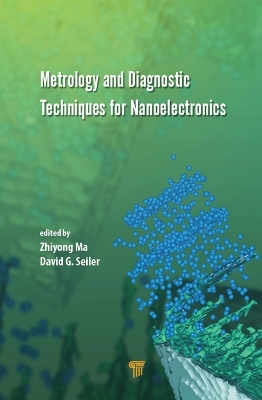
Metrology and Diagnostic Techniques for Nanoelectronics
Pan Stanford Publishing Pte Ltd (Verlag)
978-981-4745-08-6 (ISBN)
- Titel nicht im Sortiment
- Artikel merken
Zhiyong Ma received his MS degree in materials engineering from Purdue University, Indiana, and a PhD in materials science and engineering from the University of Illinois, Urbana-Champaign. He worked in thin-film metallization and processing at Digital Equipment Corporation and joined Intel’s Corporate Quality Network in 1995. Currently, he is vice president of the Technology and Manufacturing Group and director of Technology Development and Manufacturing Labs at Intel, responsible for the CQN lab network in support of silicon and assembly technology development and manufacturing, product fault diagnostics, and silicon and platform benchmarking, including strategic business planning, analytical technique development, and metrology roadmaps. Dr. Ma holds 8 patents in underbump metallization, strained silicon transistors, secured fuse technology, and silicon diagnostic techniques, has published more than 25 refereed papers, and has coauthored a book chapter on silicide technology. His research interests include thin-film kinetics, analytical techniques and metrology, and product fault diagnostics. David G. Seiler received his PhD and MS in physics from Purdue University and a BS in physics from Case Western Reserve University, Ohio. He is a fellow of the American Physical Society and a fellow of the Institute of Electrical and Electronic Engineers. In 2000, he received a Distinguished Alumni Award from Purdue University's School of Science for his contributions to and achievements in semiconductors. He served as solid state physics program director in the Materials Research Division, National Science Foundation; spent a year’s sabbatical at the MIT Francis Bitter National Magnet Laboratory; and was a regents’ professor of physics at the University of North Texas. He joined the National Institute of Standards and Technology (NIST) in 1988 and served as program analyst in the program office for the director of NIST and as materials technology group leader in the Engineering Physics Division. Currently, he is chief of the division, which provides technical leadership in measurement science research, development, and standards essential to improving US economic competitiveness for advanced manufacturing. Dr. Seiler has been the chairperson and proceedings editor of 15 international conferences or workshops. He is the coeditor and coauthor of a chapter in Semiconductors and Semimetals (1992, Vol. 36) and a coauthor of a chapter in Handbook of Optics (1995, revised 2009). His current research focus is on understanding and advancing the metrology and characterization measurements needed for the future of nanoelectronics. The results of his research have been disseminated in over 200 publications and 100 talks throughout the world.
Model-Based Scanning Electron Microscopy Critical Dimension Metrology for 3D Nanostructures. X-Ray Metrology for Semiconductor Fabrication. Advancements in Ellipsometric and Scatterometric Analysis. 3D-AFM Measurements for Semiconductor Structures and Devices. Microstructure Characterization of Nanoscale Materials and Interconnects. Characterization of the Chemistry and Mechanical Properties of Interconnect Materials and Interfaces: Impact on Interconnect Reliability. Characterization of Plasma Damage for Low-κ Dielectric Films. Defect Characterization and Metrology. 3D Electron Tomography for Nanostructures. Methodology and Challenges in Characterization of 3D Package Interconnection Materials and Processes. 3D Interconnect Characterization using Raman Spectroscopy. Optical and Electrical Nanoprobing for Circuit Diagnostics. Automated Tools and Methods for Debugging and Diagnosis.
| Erscheinungsdatum | 11.12.2016 |
|---|---|
| Zusatzinfo | 249 Illustrations, color; 452 Illustrations, black and white |
| Verlagsort | Singapore |
| Sprache | englisch |
| Maße | 152 x 229 mm |
| Gewicht | 1864 g |
| Themenwelt | Naturwissenschaften ► Physik / Astronomie ► Optik |
| Technik ► Elektrotechnik / Energietechnik | |
| Technik ► Maschinenbau | |
| ISBN-10 | 981-4745-08-1 / 9814745081 |
| ISBN-13 | 978-981-4745-08-6 / 9789814745086 |
| Zustand | Neuware |
| Informationen gemäß Produktsicherheitsverordnung (GPSR) | |
| Haben Sie eine Frage zum Produkt? |
aus dem Bereich


