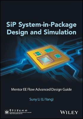
SiP System-in-Package Design and Simulation
John Wiley & Sons Inc (Verlag)
978-1-119-04593-9 (ISBN)
- Lieferbar (Termin unbekannt)
- Versandkostenfrei
- Auch auf Rechnung
- Artikel merken
An advanced reference documenting, in detail, every step of a real System-in-Package (SiP) design flow
Written by an engineer at the leading edge of SiP design and implementation, this book demonstrates how to design SiPs using Mentor EE Flow. Key topics covered include wire bonding, die stacks, cavity, flip chip and RDL (redistribution layer), Embedded Passive, RF design, concurrent design, Xtreme design, 3D real-time DRC (design rule checking), and SiP manufacture.
Extensively illustrated throughout, System in Package Design and Simulation covers an array of issues of vital concern for SiP design and fabrication electronics engineers, as well as SiP users, including:
Cavity and sacked dies design
FlipChip and RDL design
Routing and coppering
3D Real-Time DRC check
SiP simulation technology
Mentor SiP Design and Simulation Platform
Designed to function equally well as a reference, tutorial, and self-study, System in Package Design and Simulation is an indispensable working resource for every SiP designer, especially those who use Mentor design tools.
Mr. Suny Li (Li Yang) is a SiP/PCB Technical Specialist in China; he now works in AcconSys Technology Co. Ltd, (a Mentor Authorized Distributor for China). Suny has guided and consulted on dozens of SiP projects in China, accumulating plentiful experience in SiP design and simulation. Suny has 10 years' experience in and knowledge of Application Engineer for Mentor, especially in SiP/PCB design and simulation. Before this, Suny worked in the Chinese Academy of Science and SIEMENS for several years. He has more than seven years' experience in hardware design (HW system design, PCB layout, high–speed signal integrity, power integrity, EMI, etc.). In the course of his work, Suny has published papers and acquired four patents, and he continues with this work. Suny is a senior member of the Chinese Institute of Electronics (CIE) and a member of the IEEE. Suny graduated from Beijing University of Aeronautics & Astronautics (BUAA) in 2000, receiving Master's and Bachelor's degrees in Science and Technology of Aeronautics & Astronautics.
About the Author xiii
Preface xv
1 SiP Design and Simulation Platform 1
1.1 From Package to SiP 1
1.2 The Development of Mentor SiP Design Technology 5
1.3 The Mentor SiP Design and Simulation Platform 6
1.4 The Introduction of the Finished Project 16
2 Introduction to Package 19
2.1 Definition and Function of Package 19
2.2 Development of Packaging Technology 20
2.3 SiP and Related Technologies 24
2.4 The Development of the Package Market 31
2.5 Package Manufacturers 32
2.6 Bare Chip Suppliers 35
3 The SiP Production Process 37
3.1 BGA: The Mainstream SiP Package Form 37
3.2 The SiP Package Production Process 39
3.3 Three Key Elements of SiP 41
4 New Package Technologies 45
4.1 TSV (Through Silicon Via) Technology 45
4.2 Integrated Passive Device (IPD) Technology 49
4.3 Package on Package (PoP) Technology 51
4.4 Apple A8 processor – an Example of a PoP Product 55
5 SiP Design and Simulation Flow 59
5.1 SiP Design and Simulation Flow 59
5.2 Design and Simulation Process in Mentor EE Flow 61
6 Central Library 67
6.1 The Structure of the Central Library 67
6.2 Introduction to the Dashboard 68
6.3 Schematic Symbol Creation 70
6.4 Bare Chip Cell Creation 76
6.5 BGA Cell Creation 82
6.6 Part Creation 90
6.7 Create Cell Via Part 92
7 Schematic Input 97
7.1 Netlist Input 97
7.2 Basic Schematic Input 99
7.3 Schematic Input Based on DxDataBook 120
8 Multi-board Project Management and Concurrent Schematic Design 127
8.1 Multi-Board Project Management 127
8.2 Concurrent Schematic Design 130
9 Layout Creation and Setting 137
9.1 Create Layout Template 137
9.2 Create Layout Project 146
9.3 Layout-Related Setup and Operation 149
9.4 Substrate Layout 174
9.5 eDxD View 177
9.6 Input Chinese Characters in Layout 178
10 Constraint Rules Management 183
10.1 CES – Constraint Editor System 183
10.2 Scheme 185
10.3 Define Layer Stackup and Parameters 187
10.4 Net Class 188
10.5 Clearance Rules 190
10.6 Constraint Class 194
10.7 Update CES Data with Layout 200
11 Wire Bond Design 201
11.1 Wire Bond Overview 201
11.2 Bond Wire Model 203
11.3 Wire Bond Toolbar 209
12 Cavity and Chip Stack Design 229
12.1 Cavity 229
12.2 Chip Stack 239
13 Flip Chip and RDL Design 249
13.1 The Concept and Characteristics of Flip Chip 249
13.2 The RDL Concept 250
13.3 RDL Design 250
13.4 Flip Chip Design 260
14 Route and Plane 269
14.1 Routing 269
14.2 Plane 291
15 Embedded Passives Design 303
15.1 The Development of Embedded Technology 303
15.2 Process and Material for Embedded Passives 305
15.3 Resistor and Capacitor Automatic Synthesis 319
16 RF Circuit Design 331
16.1 RF SiP Technology 331
16.2 Mentor RF Design Flow 332
16.3 RF Schematic Design 333
16.4 RF Parameter Transfer Between Schematic and Layout 342
16.5 RF Layout Design 344
16.6 Connect RF Simulation Tools and Transfer Data 363
17 Concurrent Layout Design 367
17.1 Concurrent Layout Design Technology – Xtreme 367
17.2 Xtreme Configuration 369
17.3 Start Xtreme Concurrent Design 371
17.4 Matters to Note in Xtreme 375
18 3D Real-time DRC 377
18.1 Wire Model Editor 3D Display and DRC 377
18.2 3D Viewer Display and DRC 380
19 Design Review 395
19.1 Online DRC 395
19.2 Batch DRC 395
19.3 Review Hazards 401
19.4 Verify Design Library 403
20 Manufacturing Data Output 407
20.1 Drill and Gerber Data Output 407
20.2 Other Manufacturing Data Output 416
21 SiP Simulation Technology 425
21.1 SiP Simulation Technology Overview 425
21.2 Signal Integrity Simulation 426
21.3 Power Integrity Simulation 436
21.4 Thermal Analysis 443
21.5 EMI/EMC Analysis 457
21.6 Mixed-Signal Simulation Introduction 462
Reference Materials 467
Postscript and Thanks 469
Index 471
| Erscheinungsdatum | 28.09.2017 |
|---|---|
| Verlagsort | New York |
| Sprache | englisch |
| Maße | 168 x 249 mm |
| Gewicht | 953 g |
| Themenwelt | Technik ► Elektrotechnik / Energietechnik |
| ISBN-10 | 1-119-04593-2 / 1119045932 |
| ISBN-13 | 978-1-119-04593-9 / 9781119045939 |
| Zustand | Neuware |
| Haben Sie eine Frage zum Produkt? |
aus dem Bereich


