ESD (eBook)
412 Seiten
Wiley (Verlag)
978-0-470-03006-6 (ISBN)
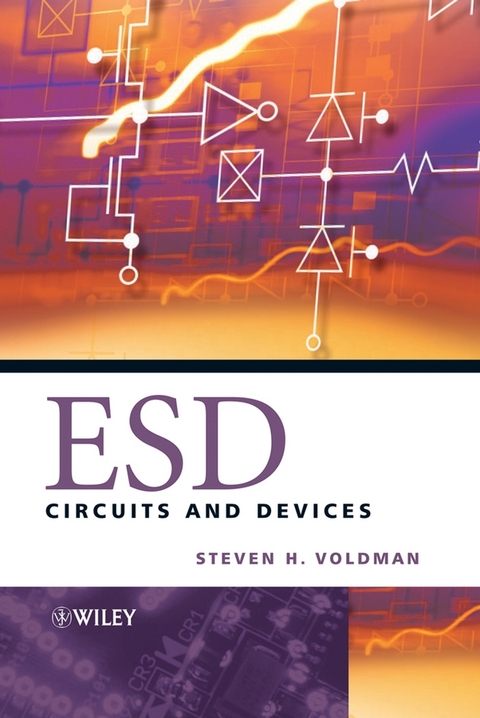
ESD Circuits and Devices provides a clear insight intothe layout and design of circuitry for protection againstelectrical overstress (EOS) and ESD. With an emphasis onexamples, this text:
* explains ESD buffering, ballasting, current distribution,design segmentation, feedback, coupling, and de-coupling ESD designmethods;
* outlines the fundamental analytical models and experimentalresults for the ESD design of MOSFETs and diode semiconductordevice elements, with a focus on CMOS, silicon on insulator (SOI),and Silicon Germanium (SiGe) technology;
* focuses on the ESD design, optimization, integration andsynthesis of these elements and concepts into ESD networks, as wellas applying within the off-chip driver networks, and on-chipreceivers; and
* highlights state-of-the-art ESD input circuits, as well as ESDpower clamps networks.
Continuing the author's series of books on ESD, this bookwill be an invaluable reference for the professional semiconductorchip and system ESD engineer. Semiconductor device andprocess development, quality, reliability and failure analysisengineers will also find it an essential tool. In addition,both senior undergraduate and graduate students in microelectronicsand IC design will find its numerous examples useful.
Dr. Steven H. Voldman received his B. S. in Engineering Science from the University of Buffalo (1979); M.S. EE (1981) and Electrical Engineer Degree (1982) from M.I.T.; MS Engineering Physics (1986) and Ph.D. EE (1991) from the University of Vermont under IBM Resident Study Fellow program. At M.I.T., he worked as a member of the M.I.T. Plasma Fusion center, and the High Voltage Research Laboratory (HVRL). At IBM, as a reliability/device engineer, his work included pioneering work in bipolar/CMOS SRAM alpha particle and cosmic ray SER simulation, MOSFET gate-induced drain leakage (GIDL) mechanism, hot electron, epitaxy/well design, CMOS latchup, and ESD. Since 1986, he was responsible for defining the IBM ESD/latchup strategy for CMOS, SOI, BiCMOS and RF CMOS, and SiGe technologies. He has authored ESD and latchup publications in the area of MOSFET scaling, device simulation, copper, low-k, MR heads, CMOS, SOI, SiGe and SiGeC technology. Voldman served as SEMATECH ESD Working Group Chairman (1996-2000), ESD Association Technical Program Chair (2000), Vice Chairman (2001), General Chairman 2002, and ESDA Board of Directors (1998-2006), International Reliability Physics Symposium ESD/Latchup Sub-Committee Chairman (2002-2006), International Physical and Failure Analysis (IPFA) Symposium ESD Sub-Committee Chairman (2003-2005), ESD Association Standard Development Chairman on Transmission Line Pulse Testing (2000-2006), ESD International Committee on Education (ICE) Asian University Liason and 'ESD on Campus' program founder, and serves in the ISQED Committee, Taiwan ESD Conference (T-ESDC) Technical Program Committee (Hsinchu, Taiwan), and the International Conference on Electromagnetic Compability (ICEMAC, Taipei, Taiwan). Voldman has provided ESD lectures for universities (e.g., M.I.T. Lecture Series, Taiwan National Chiao-Tung University (NCTU), and Singapore Nanyang Technical University (NTU)). He is a recipient of over 136 U.S. patents, over 100 publications, and recently wrote a textbook on ESD entitled ESD: Physics and Devices (John Wiley and Sons, Ltd) as well as contributing to the text 'Silicon Germanium: Modeling, Technology and Simulation,' and providing talks on patenting and invention. He has been highlighted in EE Times, Intellectual Property Law and Business and authored the first article on ESD phenomena for the October 2002 edition of Scientific American entitled 'Lightning Rods for Nano-electronics,' and Pour La Science, Le Scienze, and Swiat Nauk International editions. In 2003, Dr. Voldman was accepted as the first IEEE Fellow for ESD phenomena in semiconductors for 'contributions to electrostatic discharge protection in CMOS, SOI, and SiGe technologies.'
The scaling of semiconductor devices from sub-micron to nanometerdimensions is driving the need for understanding the design ofelectrostatic discharge (ESD) circuits, and the response of theseintegrated circuits (IC) to ESD phenomena. ESD Circuits and Devices provides a clear insight intothe layout and design of circuitry for protection againstelectrical overstress (EOS) and ESD. With an emphasis onexamples, this text: * explains ESD buffering, ballasting, current distribution,design segmentation, feedback, coupling, and de-coupling ESD designmethods; * outlines the fundamental analytical models and experimentalresults for the ESD design of MOSFETs and diode semiconductordevice elements, with a focus on CMOS, silicon on insulator (SOI),and Silicon Germanium (SiGe) technology; * focuses on the ESD design, optimization, integration andsynthesis of these elements and concepts into ESD networks, as wellas applying within the off-chip driver networks, and on-chipreceivers; and * highlights state-of-the-art ESD input circuits, as well as ESDpower clamps networks. Continuing the author's series of books on ESD, this bookwill be an invaluable reference for the professional semiconductorchip and system ESD engineer. Semiconductor device andprocess development, quality, reliability and failure analysisengineers will also find it an essential tool. In addition,both senior undergraduate and graduate students in microelectronicsand IC design will find its numerous examples useful.
Dr. Steven H. Voldman received his B. S. in Engineering Science from the University of Buffalo (1979); M.S. EE (1981) and Electrical Engineer Degree (1982) from M.I.T.; MS Engineering Physics (1986) and Ph.D. EE (1991) from the University of Vermont under IBM Resident Study Fellow program. At M.I.T., he worked as a member of the M.I.T. Plasma Fusion center, and the High Voltage Research Laboratory (HVRL). At IBM, as a reliability/device engineer, his work included pioneering work in bipolar/CMOS SRAM alpha particle and cosmic ray SER simulation, MOSFET gate-induced drain leakage (GIDL) mechanism, hot electron, epitaxy/well design, CMOS latchup, and ESD. Since 1986, he was responsible for defining the IBM ESD/latchup strategy for CMOS, SOI, BiCMOS and RF CMOS, and SiGe technologies. He has authored ESD and latchup publications in the area of MOSFET scaling, device simulation, copper, low-k, MR heads, CMOS, SOI, SiGe and SiGeC technology. Voldman served as SEMATECH ESD Working Group Chairman (1996-2000), ESD Association Technical Program Chair (2000), Vice Chairman (2001), General Chairman 2002, and ESDA Board of Directors (1998-2006), International Reliability Physics Symposium ESD/Latchup Sub-Committee Chairman (2002-2006), International Physical and Failure Analysis (IPFA) Symposium ESD Sub-Committee Chairman (2003-2005), ESD Association Standard Development Chairman on Transmission Line Pulse Testing (2000-2006), ESD International Committee on Education (ICE) Asian University Liason and "ESD on Campus" program founder, and serves in the ISQED Committee, Taiwan ESD Conference (T-ESDC) Technical Program Committee (Hsinchu, Taiwan), and the International Conference on Electromagnetic Compability (ICEMAC, Taipei, Taiwan). Voldman has provided ESD lectures for universities (e.g., M.I.T. Lecture Series, Taiwan National Chiao-Tung University (NCTU), and Singapore Nanyang Technical University (NTU)). He is a recipient of over 136 U.S. patents, over 100 publications, and recently wrote a textbook on ESD entitled ESD: Physics and Devices (John Wiley and Sons, Ltd) as well as contributing to the text "Silicon Germanium: Modeling, Technology and Simulation," and providing talks on patenting and invention. He has been highlighted in EE Times, Intellectual Property Law and Business and authored the first article on ESD phenomena for the October 2002 edition of Scientific American entitled "Lightning Rods for Nano-electronics," and Pour La Science, Le Scienze, and Swiat Nauk International editions. In 2003, Dr. Voldman was accepted as the first IEEE Fellow for ESD phenomena in semiconductors for "contributions to electrostatic discharge protection in CMOS, SOI, and SiGe technologies."
| Erscheint lt. Verlag | 3.2.2006 |
|---|---|
| Sprache | englisch |
| Themenwelt | Technik ► Elektrotechnik / Energietechnik |
| Schlagworte | Circuit Theory & Design • Electrical & Electronics Engineering • Elektrotechnik u. Elektronik • Schaltkreise - Theorie u. Entwurf |
| ISBN-10 | 0-470-03006-2 / 0470030062 |
| ISBN-13 | 978-0-470-03006-6 / 9780470030066 |
| Haben Sie eine Frage zum Produkt? |
Größe: 4,4 MB
Kopierschutz: Adobe-DRM
Adobe-DRM ist ein Kopierschutz, der das eBook vor Mißbrauch schützen soll. Dabei wird das eBook bereits beim Download auf Ihre persönliche Adobe-ID autorisiert. Lesen können Sie das eBook dann nur auf den Geräten, welche ebenfalls auf Ihre Adobe-ID registriert sind.
Details zum Adobe-DRM
Dateiformat: PDF (Portable Document Format)
Mit einem festen Seitenlayout eignet sich die PDF besonders für Fachbücher mit Spalten, Tabellen und Abbildungen. Eine PDF kann auf fast allen Geräten angezeigt werden, ist aber für kleine Displays (Smartphone, eReader) nur eingeschränkt geeignet.
Systemvoraussetzungen:
PC/Mac: Mit einem PC oder Mac können Sie dieses eBook lesen. Sie benötigen eine
eReader: Dieses eBook kann mit (fast) allen eBook-Readern gelesen werden. Mit dem amazon-Kindle ist es aber nicht kompatibel.
Smartphone/Tablet: Egal ob Apple oder Android, dieses eBook können Sie lesen. Sie benötigen eine
Geräteliste und zusätzliche Hinweise
Buying eBooks from abroad
For tax law reasons we can sell eBooks just within Germany and Switzerland. Regrettably we cannot fulfill eBook-orders from other countries.
aus dem Bereich


