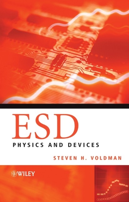
ESD
John Wiley & Sons Inc (Verlag)
978-0-470-84753-4 (ISBN)
This volume is the first in a series of three books addressing Electrostatic Discharge (ESD) physics, devices, circuits and design across the full range of integrated circuit technologies. ESD Physics and Devices provides a concise treatment of the ESD phenomenon and the physics of devices operating under ESD conditions. Voldman presents an accessible introduction to the field for engineers and researchers requiring a solid grounding in this important area. The book contains advanced CMOS, Silicon On Insulator, Silicon Germanium, and Silicon Germanium Carbon. In addition it also addresses ESD in advanced CMOS with discussions on shallow trench isolation (STI), Copper and Low K materials.
Provides a clear understanding of ESD device physics and the fundamentals of ESD phenomena.
Analyses the behaviour of semiconductor devices under ESD conditions.
Addresses the growing awareness of the problems resulting from ESD phenomena in advanced integrated circuits.
Covers ESD testing, failure criteria and scaling theory for CMOS, SOI (silicon on insulator), BiCMOS and BiCMOS SiGe (Silicon Germanium) technologies for the first time.
Discusses the design and development implications of ESD in semiconductor technologies.
An invaluable reference for EMC non-specialist engineers and researchers working in the fields of IC and transistor design. Also, suitable for researchers and advanced students in the fields of device/circuit modelling and semiconductor reliability.
Dr Steven H. Voldman received his B.S. in Engineering Science from the University of Buffalo (1979); M.S. EE (1981) and Electrical Engineer Degree (1982) from M.I.T; MS Engineering Physics (1986) and Ph.D EE (1991) from the University of Vermont under IBM's Resident Study Fellow Program. At M.I.T, he worked as a member of the M.I.T. Plasma Fusion Center, and the High Voltage Research Laboratory (HVRL). At IBM, as a reliability device engineer, his work include pioneering work in bipolar/ CMOS SRAM alpha particle and cosmic ray SER simulation, MOSFET gate-induced drain leakage (GIDL) mechanism, hot electron, epitaxy/well design, CMOS latchup, and ESD. Since 1986, he has been responsible for defining the IBM ESD/latchup strategy for CMOS, SOI, BiCMOS and RF CMOS and SiGe technologies. He has authored ESD and latchup publications in the area of MOSFET Scaling, device simulations, copper, low-k, MR heads, CMOS, SOI , Sage and SiGeC technology. Voldman served as SEMATECH ESD Working Group Chairman (1996-2000), ESD Association General Chairman and Board of Directors, International Reliability Physics (IRPS) ESD/Latchup Chairman, International Physical and Failure Analysis (IPFA) Symposium ESD Sub-Committee Chairman, ESD Association Standard Development Chairman on Transmission Line Pulse Testing, ESD Education Committee, and serves on the ISQED Committee, Taiwan ED Conference (T-ESDC) Technical Program Committee. Voldman has provided ESD lectures for universities (e.g. MIT Lecture Series, Taiwan National Chiao-Tung University, and Singapore Nanyang Technical University). He is a recipient of over 125 US patents, over 100 publications, and also provides talks on patenting, and invention. He has been featured in EE Times, Intellectual Property Law and Business and authored the first article on ESD phenomena for the October 2002 edition of Scientific American entitled Lightening Rods for Nanostructures, and Pour La Science, Le Scienze, and Swiat Nauk international editions. Dr. Voldman was recently accepted as the first IEEE Fellow for ESD phenomena in semiconductors for ' contributions to electrostatic discharge protection CMOS, SOI and SiGe technologies'.
About the Author. Preface.
Acknowledgements.
1. Electrostatics and Electrothermal Physics.
2. Electrothermal and Methods of Analysis ESD Models.
3. Semiconductor Device Physics and ESD.
4. Substrates and ESD.
5. Wells and Sub-collectors and ESD.
6. Isolation Technology and ESD.
7. Drain Engineering, Salicides and ESD.
8. Dielectrics and ESD.
9. Interconnects and ESD.
10. Silicon on Insulator (SOI) and ESD.
11. Silicon-Germanium and ESD.
12. Nanostructures and ESD.
Index.
| Erscheint lt. Verlag | 24.9.2004 |
|---|---|
| Verlagsort | New York |
| Sprache | englisch |
| Maße | 175 x 252 mm |
| Gewicht | 948 g |
| Themenwelt | Naturwissenschaften ► Physik / Astronomie ► Elektrodynamik |
| ISBN-10 | 0-470-84753-0 / 0470847530 |
| ISBN-13 | 978-0-470-84753-4 / 9780470847534 |
| Zustand | Neuware |
| Haben Sie eine Frage zum Produkt? |
aus dem Bereich


