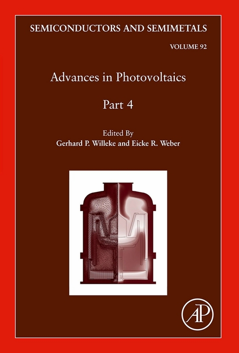
Advances in Photovoltaics: Part 4 (eBook)
192 Seiten
Elsevier Science (Verlag)
9780128010686 (ISBN)
Advances in Photovoltaics: Part Four provides valuable information on the challenges faced during the transformation of our energy supply system to more efficient, renewable energies. The volume discusses the topic from a global perspective, presenting the latest information on photovoltaics, a cornerstone technology. It covers all aspects of this important semiconductor technology, reflecting on the tremendous and dynamic advances that have been made on this topic since 1975, when the first book on solar cells written by Harold J. Hovel of IBM was published as volume 11 in the now famous series on Semiconductors and Semimetals. Readers will gain a behind the scenes look at the continuous and rapid scientific development that leads to the necessary price and cost reductions in global industrial mass-production. - Written by leading, internationally known experts on his topic- Provides an in-depth overview of the current status and perspectives of thin film PV technologies- Discusses the challenges faced during the transformation of our energy supply system to more efficient, renewable energies- Delves deep into photovoltaics, a cornerstone technolog
Silicon Crystallization Technologies
Peter Dold1 Fraunhofer CSP, Halle, Germany
1 Corresponding author: email address: peter.dold@ise.fraunhofer.de
Abstract
More than 90% of all Photovoltaic (PV) installations are based on crystalline silicon, several hundred thousand tons of which are processed by the solar industry each year. During the last few years, we have seen a huge price reduction in the polysilicon market. But still, the raw material contributes significantly to the total costs and further price reductions might be expected. Today, most polysilicon is produced by the Siemens process, but alternative routes like fluidized-bed reactors or upgraded metallurgical silicon might provide a better cost structure and thus might gain market shares.
The majority of solar silicon is crystallized by the directional solidification method (also called vertical gradient freeze method). This technique is quite robust, easy to handle, and easily scalable. Block sizes between 500 kg and 1 ton are the actual standard. The latest development is the small-grain, high-performance multi. Compared to quasi-mono (mono-like) silicon, the better cost structure and the lower process complexity of the high-performance multi are a clear advantage.
Some 40% of the silicon is crystallized as mono ingots. Right now, Czochralski (Cz) is the standard technology: 8″ or 9″ ingots of cylindrical shape and a length of 1.5–2 m are grown. Since Cz is hardly scalable to larger ingots, the challenge is to reduce cost by accelerating the process, by reducing downtime, and by making a better use of the consumables. Actual trends are multipulling, feeding, continuous pulling, or active crystal cooling to mention just some of them. In particular, for high-efficiency cell technologies like Interdigitated Back Contact (IBC) or Heterojunction with Intrinsic Thin layer (HIT), high-quality n-type material is required.
Finally, the Float-Zone (FZ) technique will be discussed. FZ ingots have at least two orders of magnitude lower oxygen levels compared to Cz material and the corresponding minority carrier lifetimes are very high. Right now, the process suffers by its complexity and the lack of affordable feed rods. Overcoming these limitations, FZ might be an interesting alternative for high-efficiency applications.
Keywords
Polysilicon feedstock
Crystallization
Czochralski growth
Float Zone
Directional solidification/vertical gradient freeze
Growth parameters
1 Silicon Feedstock
1.1 Polysilicon: The Base Material for over 90% of All Solar Cells
The roller coaster ride of the polysilicon industry during the last 10 years was quite extraordinary—even compared with the ups and downs of the semiconductor business over the last half century. The golden age of polysilicon in the years 2007–2010, when companies could make billions of dollars if they were able to deliver polysilicon at all, was followed by the severe crush in the years 2011–2012, when most of the newcomers marched into bankruptcy and disappeared. And, even some of the old ones had to fight heavily to survive. During the golden years, spot market prices had reached highs of 200–300 or even 400 US$/kg polysilicon, simply because the market was swept and the order books of the cell and module manufacturers were full. The polysilicon industry was not prepared for such a fast ramp-up, investment is high,1 and equipment could not readily be ordered. The long-established companies either have an exclusive partnership with a specific equipment manufacturer, or they make the equipment in-house. Production capacity could not easily be ramped up, but once the train was running, it also could not be stopped so easily and could not be adjusted to the then changed market situation, partly because typical polysilicon projects take several years from the financing phase all the way up to full production, and partly because the players did not want to believe that the silicon bonanza was over. The huge shortage was followed by a tremendous over supply with spot market prices as low as 14–16 US$/kg in 2013—which was below the actual production costs. Today, spot market prices leveled off around 17–18 US$/kg and no significant changes are expected for the near future.
As a consequence, all (or at least as good as all) of the new and innovative approaches for polysilicon refinement, for upgrading metallurgical silicon (an excellent review was given by Heuer, 2013), or for alternative production methods (compare Bernreuter and Haugwitz, 2010) could not find a market share and disappeared again. The traditional Chemical Vapor Deposition (CVD)-based Siemens process (Fabry and Hesse, 2012), probably not the most sophisticated technology for solar-grade-silicon production—but for sure the most matured technique, was the match winner. A good overview of the market situation and an in-depth analysis of the trends are given by Bernreuter every first or second year (Bernreuter, 2014).
Basically, two main routes might be distinguished for the refinement of polysilicon: (I) the chemical path: bringing silicon into the gas phase and purifying it by distillation, followed by thermal pyrolysis of the gaseous species; and (II) the metallurgical path, where impurities are removed from silicon by mixing it with another metal or with a slag, then let the impurities segregate into the second phase, separate the different phases somehow mechanically, and clean the surface of the silicon crystallites by chemical etching.
1.2 The Chemical Path
The Siemens process (or modified Siemens process, as many manufacturers like to call their variation) allows to produce ultrapure polysilicon, with metallic bulk impurity levels as low as a few tens of ppt (parts per trillion) or an equivalent of 10–11N. Electrically active elements (donors, acceptors) are in the ppt range and only carbon and oxygen show up in higher concentrations, where lower single-digit parts per million levels are found. For semiconductor applications, there is no alternative so far to the polysilicon produced by the Siemens process.
The Siemens process itself goes back to a patent in the late 1950s filed by the German electronics company Siemens (Reuschel, 1963; Schweickert et al., 1961), which stepped out of the polysilicon business long ago. It can be described by the following process steps:
I. Milling of the metallurgical silicon (purity: 98–99%) into millimeter/submillimeter particles.
II. Reaction between the fine silicon particles and gaseous HCl at temperatures around 300–350 °C in a fluidized-bed reactor (FBR). The reactor might be heated from the outside, but the chemical reaction is also strongly exothermic. Mainly copper is used as a catalyst. The main product is TCS (trichlorosilane, SiHCl3).
III. Fractional distillation of the TCS and the by-products, like metal chlorides, boron, and phosphorus components, and so on. The result will be ultrapure TCS.
IV. Pyrolytic decomposition of TCS in a bell-jar reactor (Fig. 1) at increased pressure (normally 6 bar) and temperatures of 1000–1150 °C (Fig. 2). High-purity polysilicon will be obtained (Fig. 3).
Steps I–III are relatively straightforward, although the installation of the hardware reaches easily the size and complexity of a huge chemical plant for typical production capacities of around 10,000 t/a. Step IV is more difficult:
– The high temperature required for the silicon deposition is rather energy intensive. The silicon rods on which the deposition takes place are directly heated by an electrical current.
– Deposition rates on these U-shaped rods are on the order of 0.5–1 mm/h (layer growth); beyond this rate, the rod morphology becomes unstable and so-called “popcorn” or “broccoli” growth takes place.
– Only part of the TCS decomposes to silicon, and a significant part reacts with the HCl formed during the deposition to STC (silicon tetrachloride, SiCl4). Decomposition of STC is too low at the typical rod temperatures in the bell-jar; therefore, it has to be removed from the reactor and has to be back-converted into TCS.
In former times, back-conversion of STC to TCS was carried out...
| Erscheint lt. Verlag | 25.6.2015 |
|---|---|
| Sprache | englisch |
| Themenwelt | Naturwissenschaften ► Physik / Astronomie ► Festkörperphysik |
| Naturwissenschaften ► Physik / Astronomie ► Quantenphysik | |
| Technik ► Elektrotechnik / Energietechnik | |
| ISBN-13 | 9780128010686 / 9780128010686 |
| Informationen gemäß Produktsicherheitsverordnung (GPSR) | |
| Haben Sie eine Frage zum Produkt? |
Kopierschutz: Adobe-DRM
Adobe-DRM ist ein Kopierschutz, der das eBook vor Mißbrauch schützen soll. Dabei wird das eBook bereits beim Download auf Ihre persönliche Adobe-ID autorisiert. Lesen können Sie das eBook dann nur auf den Geräten, welche ebenfalls auf Ihre Adobe-ID registriert sind.
Details zum Adobe-DRM
Dateiformat: EPUB (Electronic Publication)
EPUB ist ein offener Standard für eBooks und eignet sich besonders zur Darstellung von Belletristik und Sachbüchern. Der Fließtext wird dynamisch an die Display- und Schriftgröße angepasst. Auch für mobile Lesegeräte ist EPUB daher gut geeignet.
Systemvoraussetzungen:
PC/Mac: Mit einem PC oder Mac können Sie dieses eBook lesen. Sie benötigen eine
eReader: Dieses eBook kann mit (fast) allen eBook-Readern gelesen werden. Mit dem amazon-Kindle ist es aber nicht kompatibel.
Smartphone/Tablet: Egal ob Apple oder Android, dieses eBook können Sie lesen. Sie benötigen eine
Geräteliste und zusätzliche Hinweise
Buying eBooks from abroad
For tax law reasons we can sell eBooks just within Germany and Switzerland. Regrettably we cannot fulfill eBook-orders from other countries.
aus dem Bereich
