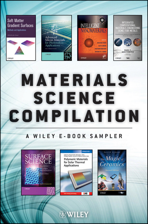
The 2013 Materials Science eBook Sampler includes select material from seven Materials Science titles. Titles are from a number of Wiley imprints including Wiley, Wiley-VCH, Wiley-American Ceramic Society, Wiley-Scrivener and Wiley-The Minerals, Metals and Materials Society. The material that is included for each selection is the book’s full Table of Contents as well as a sample chapter. If you would like to read more from these books, you can purchase the full book or e-book at your favorite online retailer.
The 2013 Materials Science eBook Sampler includes select material from seven Materials Science titles. Titles are from a number of Wiley imprints including Wiley, Wiley-VCH, Wiley-American Ceramic Society, Wiley-Scrivener and Wiley-The Minerals, Metals and Materials Society. The material that is included for each selection is the book’s full Table of Contents as well as a sample chapter. If you would like to read more from these books, you can purchase the full book or e-book at your favorite online retailer.
Chapter 1
Silicon Science and Technology as the Background of the Current and Future Knowledge Society
Sergio Pizzini
Department of Materials Science, University of Milano-Bicocca, Milan, Italy
1.1 Introduction
This introductory chapter aims to present the unique potentialities of semiconductor silicon as the substrate or the component of a variety of devices that support the development of the society in which we live today and where our sons and daughters will live, hopefully, tomorrow; taking, however, as known all the very basic physics concerning the electronic and optical properties of semiconductor silicon as well as the basic concepts concerning silicon devices [1–7]. Also, considering the number of issues that should be taken into consideration to enlighten this critical role of silicon, only a few of these, selected in a very personal, and possibly not entirely objective, manner will be discussed in full detail.
The discussion will start from the thermonuclear synthesis of silicon and will end with the properties and applications of silicon nanodots and nanowires studied today in research labs worldwide, with the consideration that silicon's uniqueness derives from its specific structural, physical and chemical properties, which make elemental silicon readily obtainable from widely diffused raw materials and directly suitable for technological applications in microelectronics, optoelectronics and photovoltaics, without neglecting high-power devices, chemical sensors and radiation detectors.
The analysis will be focused on the variety of its structural forms, which range from single crystal towards microcrystalline, nanocrystalline and amorphous, with a discontinuous change of properties that, in fact, allow a multiplicity of applications.
Also, the physics of defects in silicon will be briefly taken into consideration, in order to provide insight into its radiation hardness, which makes silicon particularly suitable in hard-radiation environments, like space and the modern hadronic colliders, as well as the role of defect engineering in modern microelectronics and optoelectronics.
Finally, a few advanced applications will be discussed.
1.2 Silicon Birth from a Thermonuclear Nucleosynthetic Process
It is well known that silicon, in the form of silicon compounds, is the main component of the earth's crust, as well as that earth has a liquid iron core. It is instead, probably, not so well known that silicon and iron are the main results of the gravitational collapse of a blue giant, a star at least eight times more massive than our sun [8]. Only with this kind of star might the thermonuclear nucleosynthetic processes driven by gravity and temperature occur within their cores, which succeed, after the combustion of hydrogen, helium and carbon (see Figure 1.1), to reach the formation of silicon (28Si) by fusion of a carbon (12C) and an oxygen nucleus (16O). The nuclear process then proceeds by the fusion of Si to (56Fe) iron. Conditions in the core then become so extreme that electron pressure is overcome and the protons are forced to react with electrons to give neutrons and neutrinos
1.1
and a neutron star is born (see Figure 1.1).
Figure 1.1 Sequence of events occurring during the final burst of a blue giant star.
The rebounding shock wave plus radiation pressure from the escaping neutrinos could also cause the outer layers of the star to explode outwards as a Type-II supernova. This condition causes a massive flux of free neutrons, and the existing nuclei are able to absorb one or more of these neutrons, undergo beta decay, absorb another neutron or neutrons, beta decay, a process that moves nuclei up the periodic table towards and past uranium. This kind of explosion disseminates a cloud of multicomponent dust in the open space, where the dust can aggregate, again under the action of gravity, giving rise to new stars and planets, these last, like the earth, with a light silica and silicate crust and a heavy iron core.
1.3 Silicon Key Properties
1.3.1 Chemical and Structural Properties
Silicon is chemically very active, it reacts in a wide range of temperatures with oxygen, metals and oxides less stable than silicon dioxide (SiO2)
1.2
1.3
1.4
(where MeSi is a metallic impurity in a substitutional or interstitial position of the silicon lattice) giving rise to the initial formation of an oxide or a surface alloy. As most of the common oxides are thermodynamically less stable than SiO2, see Figure 1.2, surface contamination of silicon by interaction with most oxide ceramics is a common event in high-temperature silicon processing.
Figure 1.2 Temperature dependence of the standard free energy of formation of selected oxides: the change of colors in the case of Al and Ca occur at the melting point of the metals (San Josè State University Ellingham diagrams web tool).
Subsequent annealing might favor the indiffusion of the metals segregated at the surface, with a definitive bulk alloying. This is one of the main technological problems encountered with silicon growth, wafering and its further processing. Metallic impurities, in turn, generate gap states that might behave as deep recombination centers for electronically or optically injected minority carriers and/or trap levels for majority carriers [9]. A key property of silicon dioxide, which will be discussed in Chapter 4, is its ability, in the form of micrometric or submicrometric precipitates, to getter metallic impurities, where gettering is a process able to trap and electrically inactivate a metallic impurity dissolved in silicon.
Gettering has been [10, 11] and still is, one of the most important applications of defect engineering, a topic and a process technology that has been steadily investigated during the past forty years and brought to success the microelectronic sector [12, 13].
Due to its high thermodynamic stability (ΔG°(298 K) = − 825.30 kJ/mol), its high dielectric constant and its compliance with the silicon surface, silicon dioxide (SiO2) behaves also as an almost perfect, impervious and electronically nonconducting membrane, which protects the silicon surface from further oxidation, acting also as a nonconducting electronic barrier. It is well known that MOS device development has been possible thanks to this property [4].
In comparison with compound semiconductors, silicon offers the advantage of being elemental, and therefore, not subject to stoichiometry deviations, which penalize in some cases the success of doping procedures in compound semiconductors.
Differently from most compound semiconductors silicon is environmentally friendly, and it does not present major decommissioning problems at the end of life of any silicon device, including photovoltaic modules.
Depending on its structure at the macro-, micro-, nanolevel, the electronic properties of the material show sensible changes.
Under atmospheric pressure at temperatures below its melting temperature at 1412°C, independently of its microscopic structure, solid silicon is a semiconductor with a cubic, diamond-like structure.
Under applied mechanical stress, silicon presents a number (at least four) of high-pressure, metastable metallic polytypes [14], with the first phase transition from the diamond structure to that of β-Sn occurring at 20 GPa. A number of additional phases might be obtained by indentation or nanoindentation [15].
In its intrinsic, undoped, state, it presents all the typical fundamental properties of elemental covalent semiconductors in terms of mechanical and thermal properties, band structure, optical properties, resistivity, electron mobility and lifetime [2]. The energy gap of silicon is 1.12 eV wide, almost at the center of the emission spectrum of the sun and therefore very suitable for solar photon harnessing.
It can be easily doped p-type and n-type with acceptor (B, Ga) and donor (P, As, Sb) substitutional impurities during the crystal growth process using a mother alloy, or during device manufacturing process using diffusion and/or ion implantation technologies. Due to the relatively small mobility of dopants, the doping profile remains almost constant during the device lifetime, with a great advantage for the long-term properties of silicon-based devices.
At the nanometric limit, under atmospheric pressure, it behaves, instead, as a quasidirect-gap semiconductor and its properties might be tuned by changing the size of the nanocrystallites, as is shown in Chapter 9.
Under atmospheric-pressure conditions, it can be grown from a liquid charge as a single-crystal ingot with the float zone and Czochralski processes or as a multicrystalline ingot with variants of the Bridgman technique, where the bulk texture depends on the crystallization conditions.
It can also be deposited, from suitable gas phases or plasma atmospheres, using chemical vapor deposition (CVD) techniques, epitaxially on a single-crystal substrate, or on nonsingle-crystal substrates, in microcrystalline, nanocrystalline or amorphous configuration, as is shown in Chapters 7 to 10.
Under specific electrochemical conditions, an array of nanocrystalline silicon dendrites might be created starting from bulk silicon, with the formation of so-called porous silicon (PS) [16–18] that presents peculiar optical emission properties, suitable both for the fabrication of light-emitting diodes (LED) and chemical and...
| Erscheint lt. Verlag | 15.2.2013 |
|---|---|
| Sprache | englisch |
| Themenwelt | Naturwissenschaften ► Chemie |
| Technik ► Maschinenbau | |
| ISBN-10 | 1-118-60584-5 / 1118605845 |
| ISBN-13 | 978-1-118-60584-4 / 9781118605844 |
| Haben Sie eine Frage zum Produkt? |
Größe: 23,7 MB
Kopierschutz: Adobe-DRM
Adobe-DRM ist ein Kopierschutz, der das eBook vor Mißbrauch schützen soll. Dabei wird das eBook bereits beim Download auf Ihre persönliche Adobe-ID autorisiert. Lesen können Sie das eBook dann nur auf den Geräten, welche ebenfalls auf Ihre Adobe-ID registriert sind.
Details zum Adobe-DRM
Dateiformat: PDF (Portable Document Format)
Mit einem festen Seitenlayout eignet sich die PDF besonders für Fachbücher mit Spalten, Tabellen und Abbildungen. Eine PDF kann auf fast allen Geräten angezeigt werden, ist aber für kleine Displays (Smartphone, eReader) nur eingeschränkt geeignet.
Systemvoraussetzungen:
PC/Mac: Mit einem PC oder Mac können Sie dieses eBook lesen. Sie benötigen eine
eReader: Dieses eBook kann mit (fast) allen eBook-Readern gelesen werden. Mit dem amazon-Kindle ist es aber nicht kompatibel.
Smartphone/Tablet: Egal ob Apple oder Android, dieses eBook können Sie lesen. Sie benötigen eine
Geräteliste und zusätzliche Hinweise
Buying eBooks from abroad
For tax law reasons we can sell eBooks just within Germany and Switzerland. Regrettably we cannot fulfill eBook-orders from other countries.
Größe: 13,7 MB
Kopierschutz: Adobe-DRM
Adobe-DRM ist ein Kopierschutz, der das eBook vor Mißbrauch schützen soll. Dabei wird das eBook bereits beim Download auf Ihre persönliche Adobe-ID autorisiert. Lesen können Sie das eBook dann nur auf den Geräten, welche ebenfalls auf Ihre Adobe-ID registriert sind.
Details zum Adobe-DRM
Dateiformat: EPUB (Electronic Publication)
EPUB ist ein offener Standard für eBooks und eignet sich besonders zur Darstellung von Belletristik und Sachbüchern. Der Fließtext wird dynamisch an die Display- und Schriftgröße angepasst. Auch für mobile Lesegeräte ist EPUB daher gut geeignet.
Systemvoraussetzungen:
PC/Mac: Mit einem PC oder Mac können Sie dieses eBook lesen. Sie benötigen eine
eReader: Dieses eBook kann mit (fast) allen eBook-Readern gelesen werden. Mit dem amazon-Kindle ist es aber nicht kompatibel.
Smartphone/Tablet: Egal ob Apple oder Android, dieses eBook können Sie lesen. Sie benötigen eine
Geräteliste und zusätzliche Hinweise
Buying eBooks from abroad
For tax law reasons we can sell eBooks just within Germany and Switzerland. Regrettably we cannot fulfill eBook-orders from other countries.
aus dem Bereich


