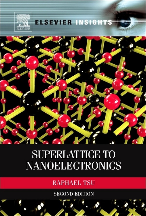
Superlattice to Nanoelectronics (eBook)
346 Seiten
Elsevier Science (Verlag)
9780080968148 (ISBN)
Dr. R. Tsu started his professional career at the Bell Telephone Laboratories, Murray Hill, NJ, 1961, working on the theory and experiments related to electron-phonon interaction in piezoelectric solids. He became a close collaborator of Leo Esaki (Nobel Laureate in 1973) at IBM T.J. Watson Research Center where he joined in 1966, working on theory and experiments of optical- and transport-properties, band structures, in solids, and material characterization. A man-made semiconductor superlattice and modulation doping were conceived jointly with Esaki, in 1969, which led to a rapid development of man-made quantum materials and quantum structures eventually evolved into the present day quantum dots. His original formulation of tunneling through multiple man-made heterojunctions is widely accepted in nearly all aspects of resonant tunneling devices reaching Tera-Hertz, thus far being the fastest device to date. The theory and experiments of man-made superlattices and resonant tunneling through a quantum well led to his outstanding contribution award from IBM Research in 1975 and later in 1985, to sharing the International New Materials Prize of the American Physical Society with Esaki and Chang. In 1979, he became the head of Materials Research at Energy Conversion Devices, Inc., in charge of the study on the formation and structure of amorphous silicon. His major contributions involve the determination of bond angle distribution from Raman scattering and optical absorption measurements and experimental determination of conductivity percolation. In 1985, he became the head of the amorphous silicon research group at the Solar Energy Research Institute (now NREL) as a principal scientist, working on amorphous Si/Ge and Si/C alloys, showing that the famous Tauc's plot may be theoretically derived without adjustable parameters. In 1975, as the recipient of the Alexander von Humboldt award, he took a year sabbatical at Max Planck Institute for Solid State Physics in
Superlattice to Nanoelectronics, Second Edition, traces the history of the development of superlattices and quantum wells from their origins in 1969. Topics discussed include the birth of the superlattice; resonant tunneling via man-made quantum well states; optical properties and Raman scattering in man-made quantum systems; dielectric function and doping of a superlattice; and quantum step and activation energy. The book also covers semiconductor atomic superlattice; Si quantum dots fabricated from annealing amorphous silicon; capacitance, dielectric constant, and doping quantum dots; porous silicon; and quantum impedance of electrons. - Written by one of the founders of this field- Delivers over 20% new material, including new research and new technological applications- Provides a basic understanding of the physics involved from first principles, while adding new depth, using basic mathematics and an explanation of the background essentials
Front Cover 1
Superlattice to Nanoelectronics 4
Copyright Page 5
Table of Contents 6
Preface 10
Introduction 14
Chapter 1 Superlattice 20
1.1 The Birth of the Man-Made Superlattice 20
1.2 A Model for the Creation of Man-Made Energy Bands 23
1.3 Transport Properties of a Superlattice 25
1.4 More Rigorous Derivation of the NDC 25
1.5 Response of a Time-Dependent Electric Field and Bloch Oscillation 29
1.6 NDC from the Hopping Model and Electric Field–Induced Localization 35
1.7 Experiments 46
1.8 Type-III Superlattice (Historically Type-II Superlattice) 52
1.9 Physical Realization and Characterization of a Superlattice 63
1.10 Summary 71
Chapter 2 Resonant Tunneling via Man-Made Quantum Well States 76
2.1 The Birth of Resonant Tunneling 76
2.2 Some Fundamentals 80
2.3 Conductance from the Tsu–Esaki Formula 85
2.4 Tunneling Time from the Time-Dependent Schrödinger Equation 86
2.5 Damping in Resonant Tunneling 95
2.6 Very Short l and w for an Amorphous QW 116
2.7 Self-Consistent Potential Correction of DBRT 118
2.8 Experimental Confirmation of Resonant Tunneling 122
2.9 Instability in RTD 123
2.10 Summary 130
Chapter 3 Optical Properties and Raman Scattering in Man-Made Quantum Systems 134
3.1 Optical Absorption in a Superlattice 134
3.2 Photoconductivity in a Superlattice 140
3.3 Raman Scattering in a Superlattice and QW 143
3.4 Summary 159
Chapter 4 Dielectric Function and Doping of a Superlattice 162
4.1 Dielectric Function of a Superlattice and a Quantum Well 162
4.2 Doping a Superlattice 166
4.3 Summary 170
Chapter 5 Quantum Step and Activation Energy 172
5.1 Optical Properties of Quantum Steps 172
5.2 Determination of Activation Energy in Quantum Wells 178
5.3 Summary 182
Chapter 6 Semiconductor Atomic Superlattice (SAS) 184
6.1 Silicon-Based Quantum Wells 185
6.2 Si-Interface Adsorbed Gas (IAG) Superlattice 186
6.3 Amorphous Silicon/Silicon Oxide Superlattice 189
6.4 Silicon–Oxygen (Si–O) Superlattice 190
6.5 Estimate of the Band-Edge Alignment Using Atomic States 195
6.6 Estimate of the Band-Edge Alignment with HOMO–LUMO 196
6.7 Estimation of Strain from a Ball-and-Stick Model 198
6.8 Electroluminescence and Photoluminescence 209
6.9 Transport through a Si–O Superlattice 214
6.10 A Si–O Superlattice and Other Si/Ge, Si/Co, Si/C Monolayer Superlattice 216
6.11 Summary 219
Chapter 7 Si Quantum Dots 222
7.1 Energy States of Silicon Quantum Dots 222
7.2 Resonant Tunneling in Silicon Quantum Dots 229
7.3 Slow Oscillations and Hysteresis 235
7.4 Avalanche Multiplication from Resonant Tunneling 243
7.5 Influence of Light and Repeatability under Multiple Scans 247
7.6 Many Body Effects in Coupled Quantum Dots 249
7.7 Summary 251
Chapter 8 Capacitance, Dielectric Constant, and Doping Quantum Dots 254
8.1 Capacitance of Silicon Quantum Dots 254
8.2 Dielectric Constant of a Silicon Quantum Dot 263
8.3 Doping a Silicon Quantum Dot 272
8.4 Capacitance: Spatial Symmetry of Discrete Charge Dielectric 277
8.5 Summary 281
Chapter 9 Porous Silicon 286
9.1 Porous Silicon: Light-Emitting Silicon 286
9.2 PSi: Other Applications 291
9.3 Summary 293
Chapter 10 Some Novel Devices 296
10.1 Field Emission with Quantum Well and Nanometer Thick Multilayer Structured Cathode 296
10.2 Saturation Intensity of PbS QDs 301
10.3 Multipole Electrode Heterojunction Hybrid Structures 305
10.4 Some Fundamental Issues: Mainly Difficulties 309
10.5 Comments on Quantum Computing 311
10.6 Recent Activities in Superlattice 312
10.7 Graphene Adventure 315
10.8 Summary 318
Chapter 11 Quantum Impedance of Electrons 324
11.1 Landauer Conductance Formula 324
11.2 Electron Quantum Waveguide 325
11.3 Wave Impedance of Electrons 329
11.4 Summary 338
Chapter 12 Why Super and Why Nano? 340
12.1 Finite Solid, Giant Molecule, and Composite 340
12.2 Generalization of Superlattices into Components 340
12.3 QDs as Individual Components 342
12.4 Size Requirements 342
12.5 Superlattice and the World of Nano 343
12.6 Some New Opportunities 344
12.7 A Word of Caution 345
| Erscheint lt. Verlag | 22.10.2010 |
|---|---|
| Sprache | englisch |
| Themenwelt | Naturwissenschaften ► Chemie |
| Naturwissenschaften ► Physik / Astronomie ► Festkörperphysik | |
| Technik ► Bauwesen | |
| Technik ► Elektrotechnik / Energietechnik | |
| Technik ► Maschinenbau | |
| ISBN-13 | 9780080968148 / 9780080968148 |
| Informationen gemäß Produktsicherheitsverordnung (GPSR) | |
| Haben Sie eine Frage zum Produkt? |
Kopierschutz: Adobe-DRM
Adobe-DRM ist ein Kopierschutz, der das eBook vor Mißbrauch schützen soll. Dabei wird das eBook bereits beim Download auf Ihre persönliche Adobe-ID autorisiert. Lesen können Sie das eBook dann nur auf den Geräten, welche ebenfalls auf Ihre Adobe-ID registriert sind.
Details zum Adobe-DRM
Dateiformat: EPUB (Electronic Publication)
EPUB ist ein offener Standard für eBooks und eignet sich besonders zur Darstellung von Belletristik und Sachbüchern. Der Fließtext wird dynamisch an die Display- und Schriftgröße angepasst. Auch für mobile Lesegeräte ist EPUB daher gut geeignet.
Systemvoraussetzungen:
PC/Mac: Mit einem PC oder Mac können Sie dieses eBook lesen. Sie benötigen eine
eReader: Dieses eBook kann mit (fast) allen eBook-Readern gelesen werden. Mit dem amazon-Kindle ist es aber nicht kompatibel.
Smartphone/Tablet: Egal ob Apple oder Android, dieses eBook können Sie lesen. Sie benötigen eine
Geräteliste und zusätzliche Hinweise
Buying eBooks from abroad
For tax law reasons we can sell eBooks just within Germany and Switzerland. Regrettably we cannot fulfill eBook-orders from other countries.
aus dem Bereich
