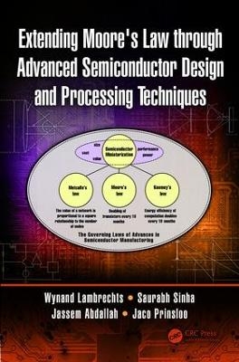
Extending Moore's Law through Advanced Semiconductor Design and Processing Techniques
Crc Press Inc (Verlag)
978-0-8153-7074-1 (ISBN)
Traditional and modern photolithography, the primary limiting factor of Moore’s law
Innovations in semiconductor manufacturing that makes current generation CMOS processing possible
Multi-disciplinary technologies that could drive Moore's law forward significantly
Design principles for microelectronic circuits and components that take advantage of technology miniaturization
The semiconductor industry economic market trends and technical driving factors
The complexity and cost associated with technology scaling have compelled researchers in the disciplines of engineering and physics to optimize previous generation nodes to improve system-on-chip performance. This is especially relevant to participate in the increased attractiveness of the Internet of Things (IoT). This book additionally provides scholarly and practical examples of principles in microelectronic circuit design and layout to mitigate technology limits of previous generation nodes. Readers are encouraged to intellectually apply the knowledge derived from this book to further research and innovation in prolonging Moore’s law and associated principles.
Johannes Wynand Lambrechts, SMIEEE, obtained his B.Eng., M.Eng., and Ph.D. degrees in Electronic Engineering from the University of Pretoria (UP), South Africa. He achieved his M.Eng. with distinction. He has authored 2 publications in peer-reviewed journals and has presented at various local and international conferences. Wynand is the lead author on two books in the fields on sustainable energy and in microelectronic engineering, published by an international publisher. He has co-authored two contributing chapters in another book in the field of green energy and technology. He previously held a position as an electronic engineer at Denel Dynamics, a state-owned company in South Africa. He is currently employed by SAAB Grintek Defence, and is also serving as a part-time research associate at the University of Johannesburg (UJ), South Africa. Saurabh Sinha, PhD(Eng), Pr Eng, SMIEEE, FSAIEE, FSAAE, Prof Sinha obtained his B. Eng, M. Eng and Ph.D. degrees in Electronic Engineering from the University of Pretoria (UP). As a published researcher, he has authored or co-authored over 110 publications in peer-reviewed journals and at international conferences. Prof Sinha served UP for over a decade; his last service being as Director of the Carl and Emily Fuchs Institute for Microelectronics, Department of Electrical, Electronic and Computer Engineering. On 1 October 2013, Prof Sinha was appointed as Executive Dean of the Faculty of Engineering and the Built Environment (FEBE) at the University of Johannesburg (UJ). Prof Sinha is currently the UJ Deputy Vice-Chancellor: Research and Internationalisation. Among other leading roles, Prof Saurabh Sinha also served the IEEE as a Board of Director and IEEE Vice-President: Educational Activities. Jassem Abdallah received his BSc in Chemical Engineering from The University of Texas at Austin with honors (undergraduate research thesis), and both his MSc and PhD in Chemical Engineering from the Georgia Institute of Technology. He completed postdoctoral research assignments at the Georgia Institute of Technology, the IBM Corporation, and the University of Johannesburg. His research background spans both Materials Science Engineering and Process Development Engineering, with a focus on semiconductor technology and organic electronic applications. He has several years of research experience working in both academic-scale, 100 mm class 100 cleanroom facilities as well as state-of-the-art 300 mm class 10 semiconductor R&D facilities. Jassem Abdallah's research focuses on the development of processes and functional materials for microelectronics applications. He has publications, patents, and invention disclosures in the fields of advanced semiconductor patterning via Directed Self Assembly (DSA); novel methods of processing thin films containing functional materials; and chemical surface modification of polymers, thin films, and substrates. Jaco Prinsloo received his B.Eng in Electronic Engineering from the University of Pretoria in 2015. He is currently employed as an embedded engineer and software developer, where his work focuses on the development of cryptographic technology.
Chapter 1 The Driving Forces Behind Moore’s Law and Its Impact on Technology Chapter 2 The Economics of Semiconductor Scaling Chapter 3 The Importance of Photolithography for Moore’s Law Chapter 4 Photolithography Enhancements Chapter 5 Future Semiconductor Devices: Exotic Materials, Alternative Architectures and Prospects Chapter 6 Microelectronic Circuit Thermal Constrictions Resulting from Moore’s Law Chapter 7 Microelectronic Circuit Enhancements and Design Methodologies to Facilitate Moore’s Law – Part I Chapter 8 Microelectronic Circuit Enhancements and Design Methodologies to Facilitate Moore’s Law – Part II Chapter 9 The Evolving and Expanding Synergy Between Moore’s Law and the Internet-of-Things Chapter 10 Technology Innovations Driven by Moore’s Law
| Erscheinungsdatum | 19.09.2018 |
|---|---|
| Zusatzinfo | 79 Tables, black and white; 20 Illustrations, color; 105 Illustrations, black and white |
| Verlagsort | Bosa Roca |
| Sprache | englisch |
| Maße | 156 x 234 mm |
| Gewicht | 540 g |
| Themenwelt | Informatik ► Weitere Themen ► Hardware |
| Technik ► Elektrotechnik / Energietechnik | |
| ISBN-10 | 0-8153-7074-1 / 0815370741 |
| ISBN-13 | 978-0-8153-7074-1 / 9780815370741 |
| Zustand | Neuware |
| Haben Sie eine Frage zum Produkt? |
aus dem Bereich


