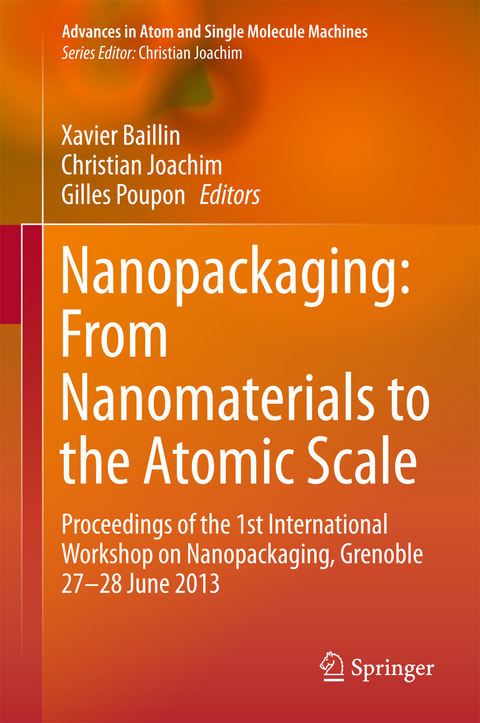
Nanopackaging: From Nanomaterials to the Atomic Scale (eBook)
VIII, 189 Seiten
Springer International Publishing (Verlag)
978-3-319-21194-7 (ISBN)
Xavier BAILLIN is CEA senior expert in the field of micro devices packaging. After twenty years dedicated to address basic research focused on the relationship between microstructure and mechanical behavior of different industrial alloys, he joined Léti in 2003 where he has been in charge of wafer level packaging activity. He has specially contributed to the development of technologies dedicated to atmosphere controlled packaging for MEMS and also in 3D integration technologies. Xavier is the co-author of about 40 publications and 20 patents. He is currently involved in a flagship project launched by CEA in 2013 and focused on bio-inspired solutions development for 3D construction at the nanometric scale.
Gilles Poupon (IEEE M'05, SM'10) received his M.S. in Electrochemistry in 1985. He joined CEA-LETI, Grenoble, France, in 1987 where he has been Director of Strategic Programs on Advanced Packaging for 10 years and is now Scientific Advisor. Gilles Poupon is a member of the Board of Governors of the IEEE Components Packaging and Manufacturing Technology Society (CPMT) and Technical Director of the International Microelectronics and Packaging Society France (IMAPS). Additionally, Gilles is Scientific Advisor of EURIPIDES (European cluster on packaging) and member of ITRS Assembly & Packaging Technical Working Group and European Branch of JISSO working group. Gilles Poupon has published two books and he has authored 3 chapters of books and co-authored and authored over 50 proceedings papers and journal papers. He has more than 10 patents in the field of advanced packaging, micro systems technologies and 3D integration.
Christian JOACHIM is CNRS Director of Research, Nanosciences group at CEMES/CNRS and adjunct Professor of Quantum Physics at Sup'Aero (ISAE) Toulouse. In Singapore, he is A*STAR VIP at IMRE on atom technology and head of the WPI MANA-NIMS satellite in Toulouse. He coordinated European projects like 'Bottom-up Nanomachines' and 'Pico-Inside'. He is currently coordinating the large European integrated project AtMol (2011-2014) to build the first ever molecular chip. He is the author of more than 230 scientific publications (h=51) and has presented over 310 invited talks on electron transfer through a molecule, STM and Atomic Force Microscopy (AFM) image calculations, tunnel transport through a molecule, molecular devices, nanolithography and single molecule machines. His book: 'Nanosciences, the invisible revolution' (World Scientific, 2009) is presenting the history of Nanosciences and its political drawbacks to a general public.
Xavier BAILLIN is CEA senior expert in the field of micro devices packaging. After twenty years dedicated to address basic research focused on the relationship between microstructure and mechanical behavior of different industrial alloys, he joined Léti in 2003 where he has been in charge of wafer level packaging activity. He has specially contributed to the development of technologies dedicated to atmosphere controlled packaging for MEMS and also in 3D integration technologies. Xavier is the co-author of about 40 publications and 20 patents. He is currently involved in a flagship project launched by CEA in 2013 and focused on bio-inspired solutions development for 3D construction at the nanometric scale.Gilles Poupon (IEEE M’05, SM’10) received his M.S. in Electrochemistry in 1985. He joined CEA-LETI, Grenoble, France, in 1987 where he has been Director of Strategic Programs on Advanced Packaging for 10 years and is now Scientific Advisor. Gilles Poupon is a member of the Board of Governors of the IEEE Components Packaging and Manufacturing Technology Society (CPMT) and Technical Director of the International Microelectronics and Packaging Society France (IMAPS). Additionally, Gilles is Scientific Advisor of EURIPIDES (European cluster on packaging) and member of ITRS Assembly & Packaging Technical Working Group and European Branch of JISSO working group. Gilles Poupon has published two books and he has authored 3 chapters of books and co-authored and authored over 50 proceedings papers and journal papers. He has more than 10 patents in the field of advanced packaging, micro systems technologies and 3D integration.Christian JOACHIM is CNRS Director of Research, Nanosciences group at CEMES/CNRS and adjunct Professor of Quantum Physics at Sup’Aero (ISAE) Toulouse. In Singapore, he is A*STAR VIP at IMRE on atom technology and head of the WPI MANA-NIMS satellite in Toulouse. He coordinated European projects like "Bottom-up Nanomachines" and “Pico-Inside”. He is currently coordinating the large European integrated project AtMol (2011-2014) to build the first ever molecular chip. He is the author of more than 230 scientific publications (h=51) and has presented over 310 invited talks on electron transfer through a molecule, STM and Atomic Force Microscopy (AFM) image calculations, tunnel transport through a molecule, molecular devices, nanolithography and single molecule machines. His book: “Nanosciences, the invisible revolution” (World Scientific, 2009) is presenting the history of Nanosciences and its political drawbacks to a general public.
Preface 6
Contents 8
1 Utilization of Peridynamic Theory for Modeling at the Nano-Scale 10
Abstract 10
1 Introduction 10
2 Peridynamic Theory 11
2.1 Peridynamic Formulation 11
2.2 Numerical Solution 14
2.3 Definition of Contact in Peridynamics 16
2.4 Peridynamic Formulation at Nano-Scale: Buffer Zone Approach 16
3 Wave Dispersion in Peridynamics 17
4 Demonstration Problems 19
4.1 Nano-Indentation 19
4.2 Single-Layer Graphene Failure 19
4.3 Multi-Layer Graphene Failure 22
5 Conclusions 24
References 25
2 DNA Metallization Processes and Nanoelectronics 26
Abstract 26
1 Introduction 26
2 Why Is It Necessary to Metallize DNA? 27
3 The DNA Metallization Process 28
4 Sequence-Selective DNA Metallization 32
5 Applications of DNA Metallization in Nanoelectronics 36
6 Conclusion 39
References 39
3 Evaluation of Leakage Current in 1-D Silicon Dangling-Bond Wire Due to Dopants 42
Abstract 42
1 Introduction 43
2 Computational Details 44
3 Results 45
4 Summary and Conclusions 47
Acknowledgments 47
References 48
4 Direct Integration of Carbon Nanotubes in Si Microsystems 50
Abstract 50
1 Introduction 51
2 Experimental 53
2.1 Design 53
2.2 Synthesis and Characterization 55
3 Results and Discussion 56
3.1 Design 56
3.2 CNT Synthesis 58
3.3 Effect of Applied Electric Field 61
3.4 Electrical Properties of Si--CNT--Si Systems 62
3.5 Gas Sensing and Functionalization 64
4 Conclusion 65
Acknowledgments 66
References 66
5 Nanopackaging Requests for Atomic Scale Circuits and Molecule-Machines 68
Abstract 68
1 Introduction 68
2 Atomic Scale Surface Preparation 69
3 Circuit Architecture for the Atomic Scale 74
4 Interconnects 79
5 Nanopackaging 83
6 Conclusion 87
Acknowledgments 87
References 88
6 Single-Crystal Au Triangles as Reconfigurable Contacts for Atomically Smooth Surfaces: Ultra-High Vacuum Transfer-Printing 91
Abstract 91
1 Introduction 92
2 Ultra-High Vacuum-Compatible Transfer-Printer 92
3 Transfer-Printing in UHV 95
3.1 MoS2 Pillar Fabrication 95
3.2 Characterization of the Transfer-Printed Samples 95
4 Conclusion 99
Acknowledgments 99
References 99
7 Site-Selective Self-Assembly of Nano-Objects on a Planar Substrate Based on Surface Chemical Functionalization 100
Abstract 100
1 Introduction 100
2 Nanoparticle Binding 102
2.1 Electrostatic Interaction 103
2.1.1 Using Intrinsic Material Properties 103
2.1.2 Using Surface Functionalization 104
2.2 Covalent Binding 105
2.3 Biomolecular Recognition 106
2.4 Nanoparticle Binding Strategies: Summary and Comparison 107
3 Chemical Patterning 109
3.1 Microcontact Printing 110
3.2 Masked Functionalization: ``SAM Lift-off'' 111
3.3 Local Modifications of a Homogeneous Surface 112
3.4 Chemical Pattern Based on Different Substrate Materials 113
3.5 Chemical Patterning Strategies: Summary and Comparison 114
4 Conclusion 115
Acknowledgements 116
References 116
8 Silicon Technologies for Nanoscale Device Packaging 120
Abstract 120
1 Introduction 120
2 Specifications for Atomic-Scale Device Packaging 122
3 Technological Steps 124
3.1 Surface Smoothing and Temporary Protection 124
3.2 Nanoscale Via Achievement by FIB 124
3.2.1 Backside Deep Cavity Processing 124
3.2.2 FIB Tools 126
3.2.3 Development of the Nanovia Etching and Filling Processes 126
3.3 Nanopads Processing 131
3.3.1 Interconnection Resistance Calculation 132
3.3.2 Nanopad Design 135
3.3.3 Nanopads Impact on Surface Reconstruction and Bonding 138
4 Summary and Conclusion 140
Acknowledgments 141
References 141
9 Designing Carbon Nanotube Interconnects for Radio Frequency Applications 143
Abstract 143
1 Introduction 144
2 Common RF Measurements of CNT 144
3 Design and Fabrication of Flip Chip Structure for High-Frequency Measurement 146
4 Flip Chip Modeling by Electromagnetic/Analytical Approach 150
4.1 Modeling of Flip Chip Device 151
4.1.1 EM Modeling of the Flip Chip Device Without the Interconnections 151
4.1.2 Analytical Modeling of the Two Interconnected Bundles of CNTs 151
4.2 Parametric Study of the Flip Chip Using the Hybrid EM/Analytical Model 154
4.2.1 Parametric Study on the CNT Resistance RCNT 156
4.2.2 Parametric Study on the CNT Contact Resistance RCNT-CNT 157
4.2.3 Parametric Study on the CNT Density (NMWCNT) 158
5 Discussion and Future Works 158
References 159
10 Packaging of Buckyballs/Buckytubes in Transparent Photo-Active Inorganic Polymers: New Hope in the Area of Electronics and Optoelectronics 161
Abstract 161
1 Introduction 162
2 Experimental 163
2.1 Material's Synthesis 163
2.2 Methods 163
3 Results and Discussions 164
3.1 SWCNT/Inorganic Glass Composite: Stress-Induced Metallization of SWCNTs in the Host and Its Application as Transparent Electrode 164
3.2 Photo-Induced Charge Separation in C60 or SWCNT/Glass Composites 171
3.2.1 C60/Glass Composite: Light-Induced Absorption (LIA) and Light-Induced ESR (LIESR) Studies 171
3.2.2 SWCNT/Glass Composite 175
Acknowledgments 178
References 178
11 Novel Nanostructured Passives for RF and Power Applications: Nanopackaging with Passive Components 180
Abstract 180
1 Introduction 180
2 Nanoscale 3D Integrated Passive Devices (3D IPDs) 183
3 Nanoscale Power Components 183
3.1 Power Inductors 183
3.2 Power Capacitors 185
4 Nanoscale RF Components 188
4.1 RF Capacitors 188
4.2 RF Inductors 189
4.3 Filters 191
4.4 Antennas 191
5 Summary 191
References 192
| Erscheint lt. Verlag | 6.8.2015 |
|---|---|
| Reihe/Serie | Advances in Atom and Single Molecule Machines | Advances in Atom and Single Molecule Machines |
| Zusatzinfo | VIII, 189 p. 124 illus., 47 illus. in color. |
| Verlagsort | Cham |
| Sprache | englisch |
| Themenwelt | Naturwissenschaften ► Biologie |
| Naturwissenschaften ► Chemie ► Physikalische Chemie | |
| Technik | |
| Schlagworte | Atom Tech • Automically Precise Manufacturing • Carbon Nanotubes • Nano-device • Nano-packaging • Scanning Probe Microscopy • Surface Engineering |
| ISBN-10 | 3-319-21194-3 / 3319211943 |
| ISBN-13 | 978-3-319-21194-7 / 9783319211947 |
| Haben Sie eine Frage zum Produkt? |
Größe: 8,2 MB
DRM: Digitales Wasserzeichen
Dieses eBook enthält ein digitales Wasserzeichen und ist damit für Sie personalisiert. Bei einer missbräuchlichen Weitergabe des eBooks an Dritte ist eine Rückverfolgung an die Quelle möglich.
Dateiformat: PDF (Portable Document Format)
Mit einem festen Seitenlayout eignet sich die PDF besonders für Fachbücher mit Spalten, Tabellen und Abbildungen. Eine PDF kann auf fast allen Geräten angezeigt werden, ist aber für kleine Displays (Smartphone, eReader) nur eingeschränkt geeignet.
Systemvoraussetzungen:
PC/Mac: Mit einem PC oder Mac können Sie dieses eBook lesen. Sie benötigen dafür einen PDF-Viewer - z.B. den Adobe Reader oder Adobe Digital Editions.
eReader: Dieses eBook kann mit (fast) allen eBook-Readern gelesen werden. Mit dem amazon-Kindle ist es aber nicht kompatibel.
Smartphone/Tablet: Egal ob Apple oder Android, dieses eBook können Sie lesen. Sie benötigen dafür einen PDF-Viewer - z.B. die kostenlose Adobe Digital Editions-App.
Zusätzliches Feature: Online Lesen
Dieses eBook können Sie zusätzlich zum Download auch online im Webbrowser lesen.
Buying eBooks from abroad
For tax law reasons we can sell eBooks just within Germany and Switzerland. Regrettably we cannot fulfill eBook-orders from other countries.
aus dem Bereich


